Ronito6
Super Member
padding resistors
track padding resistors
Is this a resistor directly sharing a trace with a leg of a trimpot? I never heard this term before.

padding resistors
track padding resistors
Is this a resistor directly sharing a trace with a leg of a trimpot? I never heard this term before.
Yes it is basically the resistor connected in series to the trim pot.
Padding resistors are mainly used for attenuation if i am not wrong.
The value of this resistor in the AU-X11 and the AU-X1 are the same, the resistors are rated at 5.6kΩ, and denoted R17 in the AU-X11 and .(R73,R74) in the AU-X1.
Basically decreasing the resistance using the trim pot, does not help us attain the required calibration value which is -11V.
With the trim pot set to null or zero resistance the maximum value you get across test points in my case at least is -10.5V and it never fails to increase beyond that..
So we decrease the value of the resistor in series with the trim pot, as the circuit sees a net resistance from trim pot along with the resistor in series.
Decreasing it to 3.9kΩ just as John did, is a good way to go about this, it will compensate for the voltage, and then you can increase the pot to have precise control and set it to the required -11V.

A couple of things...
How are you altering the input signal to the pre-amp? it seems like you are using the front panel gain controls - try using the signal generator output level control. Note that the differences you see could be caused by dirty power amp level control pots?
Also didn't you say that in one channel you have the MJ211xx sacrificial OP transistors, and in the other channel the original OP transistors? - I don't think this imbalance you see is of much consequence - at least not until you have completed the reconditioning - lots of possible reasons.
And lastly
You can't compare 'restored' with 'unrestored' and expect there to be no difference!
 , i have replaced the Green Hitachi Relay with NEC.


Nice work Ron !Nice!!
Baby that new reed relay. They are not the most rugged component. I burned mine out by experimenting with FETs on my old AU-X1's EQ boards.
A replacement for one is dicussed here.
The amp is sounding so much better than before that I hardly don’t get the feel to tear it apart for reworking the other pending driver board.

You have posted interesting pictures of the underside of the PSU/protection board.
I have yet to get a proper look at the underside of the one I am doing.

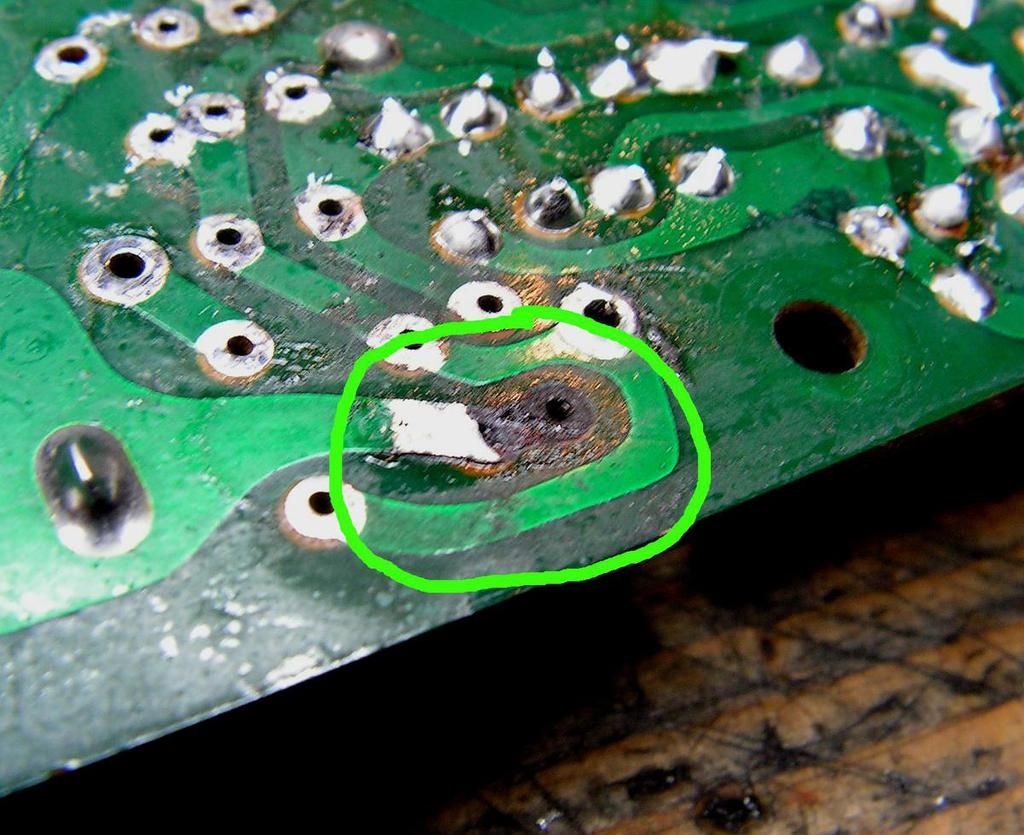
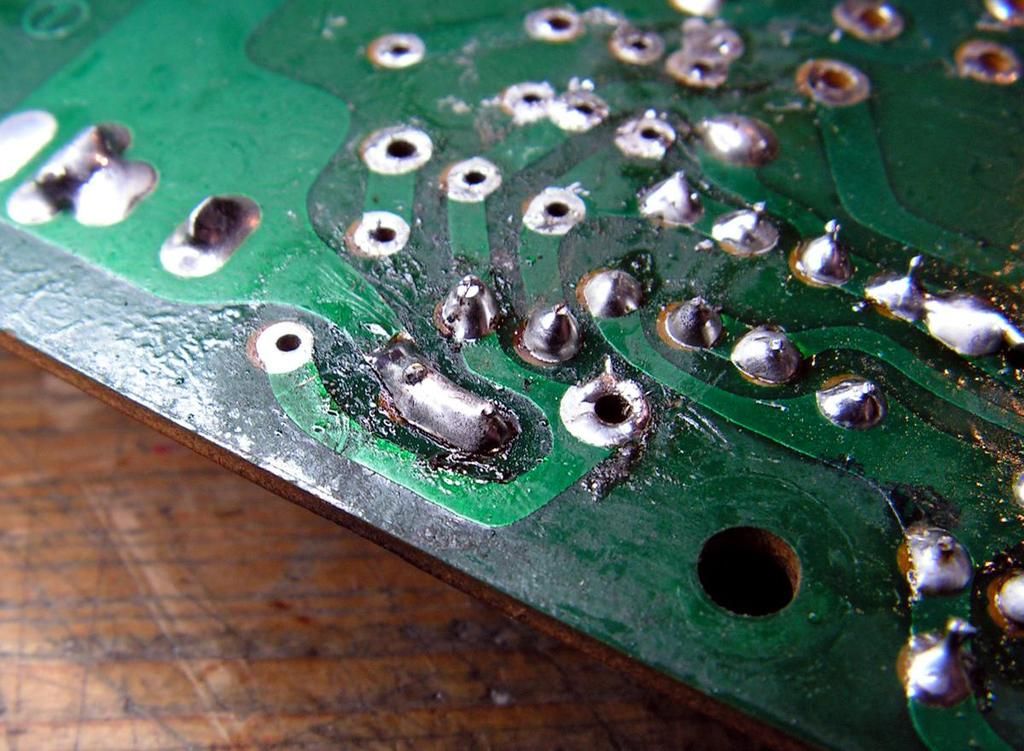
Looks neat and clean, as usual you seem to be the database of information when it comes to a restore.I'd go the Kale route, using copper shielding foil and JB Weld Highheat adhesive.
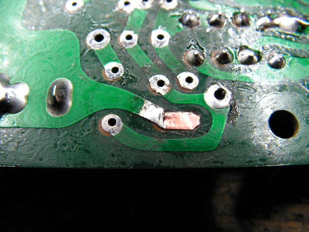
Here is a Kale PCB repair from http://audiokarma.org/forums/index....-110-volt-9090-receiver-to-the-220vac.714437/
Lovely eh?
- Clean the area to receive the adhesive.
- Apply the adhesive.
- Apply the copper patch.
- Apply low tack masking tape over the patch.
- Put an eraser or whatever can evenly apply pressure to the area.
- Then clamp the eraser (for example) in place.
- Wait 24 hours.
- Remove the clamp, eraser, and tape. Carefully clean / scrape away excess adhesive.
- Apply solder.