
One more thing to add to my previous post on my 700-T. I increased the Main Power Cap to 3300uf 63V and the Coupling caps to 2200uf 63v. IIRC the Main was 2500uf @ 55v and the couplers were 1200uf @ 55v. With the FISHER's I have a habit of going up 1-2 values (to the next thousand or as close to it I can) and keeping the voltages the same or as close as I can at the next higher voltage.

You are using an out of date browser. It may not display this or other websites correctly.
You should upgrade or use an alternative browser.
You should upgrade or use an alternative browser.
Fisher 600-T Restorations
- Thread starter fred soop
- Start date
fred soop
Super Member
One more thing to add to my previous post on my 700-T. I increased the Main Power Cap to 3300uf 63V and the Coupling caps to 2200uf 63v. IIRC the Main was 2500uf @ 55v and the couplers were 1200uf @ 55v. With the FISHER's I have a habit of going up 1-2 values (to the next thousand or as close to it I can) and keeping the voltages the same or as close as I can at the next higher voltage.
The coupling cap increase will get you down to 9 Hz for the -3 dB point with 8 ohm speakers (18 Hz at 4 ohms). So, at 20 Hz, it will be just under 1 dB down. However, I'd bump the main filter to 4400 μf or better (double the size of the output cap), because that also becomes part of the signal path during the positive part of the signal and it has to handle 2 channels with low frequencies generally being in phase.
I'll throw these values in the simulator sometime this week and see what difference the larger filter would have. For simulation of one channel, I use half the power supply filter value.
Last edited:
fred soop
Super Member
Fred, that statement brings a smile to my face,for 30 years I worked in the Teleco industry and back when I was working CO install's we also had cable reel remnants left. We had great time splitting up lot's of 4/0 cable for scrap, always a nice bonus $$$ at the end of a large job selling the left over copper.
I still have a box or two of wax string, tie wraps, jumper wire left so I guess I still have a few more years left
Do you remember the GTE lenkurt magazine? I always enjoyed reading those and still have many in storage.
Great thread.
We only took the multi conductor stuff. No heavy copper. There were warnings about not messing with the 3 "C"s. Don't mess with their cash, their copper, or their c***. In fact, a dime left on the table in a phone booth was considered company property and if one was caught pocketing that dime, it was grounds for termination.
Never knew of the GTE Lenkurt magazine but we certainly saw a LOT of Lenkurt.
Audio related story (but not Fisher): We had one old timer that would talk very loud on the phone. Being an old timer, he also had 4 weeks vacation. So, when he was gone, I (with everyones blessing) modified his phone. Sidetone is where you hear your own voice in the earpiece. The modification was to remove most of the sidetone attenuation so he would hear himself louder. It worked.
Someone once left him a message to call but left his own number instead of theirs. After a week, he walked over and said, "I figured I should just come over and talk to you in person because every time I try to call you back, the line is busy."
fred soop
Super Member
Fast Forward to 2005 and return of the 600-T (38215G)
In 2005, the Fisher 600-T was again in my possession. While not state of the art by current standards, the tuner was fairly decent and the analog tuning has some advantages over digital. The mechanical layout is very good and the front panel has a good arrangement and selection of controls and switches. The edge lighted dial with the red light in the pointer is very classy. The metal cages look much more expensive than those used on later units. This was also the only Fisher receiver, tube or transistor, to use barrier style terminal blocks on the rear panel rather than the cheaper phenolic strips. The 1974 power amplifier rebuild still worked but could easily be improved as well as the control preamp and phono preamp.
Tuner improvements could be a moot issue because maybe 3 of the 59 receivable stations have programming or technical quality that could benefit from anything above a cheap table radio, but we'll proceed anyway.
Restoration Decisions
When working on a vintage unit such as this, one must make a decision. Should it be repaired to original, meaning that it can probably only be used occasionally to demonstrate that it still works? Should it be restored to original but with improvements that will make it suitable for daily operation? Or, should it be totally redesigned, maintaining only the original appearance? Equivalent to restoring a 1957 Chevy body but installing a modern engine and transmission. My decision was to do the 3rd option, at least for the amplifier sections, especially since the power amplifier was no longer original. In other words, "What could Avery do today?"
To The Bench
This 600-T sat in Florida weather from 1979 to 2005 and dad didn't use much air conditioning after mom died in 1991. So, there were some humidity issues to deal with. Fortunately, there was no rust other than on the edges of a few rivets, but much of the dust had become caked due to being soaked with moisture. BTW, dad must have died prematurely. He did have a lot of leftover wire when I cleaned out the house. However, most of it looked like it expired before he did.
The unit powered up and the amplifier sections worked as well as they did over 30 years ago but the tuner was dead. This was quickly traced to an open high voltage winding on the power transformer. Fortunately, that is the outermost winding on this particular transformer, except for the small 6.3 volt winding that does not cover a full layer. The transformer was opened and the winding was tapped for a reduced high voltage. Changing a few resistors to compensate for the reduced voltage put the tuner back in operation but there was no stereo. This was traced to the 19 kHz to 38 kHz doubler circuit but replacement of all accessible parts did not fix the problem. It was considered that the problem might be one of the coils and there would be no readily available replacement. (Note: Problem was found and was in a completely different location. Details when we get there.)
The front panel is maybe 8 out of 10 cosmetically and has some missing plating on the top edge that was missing when new.
next: The eBay 600-T (43453K)
The coupling cap increase will get you down to 9 Hz for the -3 dB point with 8 ohm speakers (18 Hz at 4 ohms). So, at 20 Hz, it will be just under 1 dB down. However, I'd bump the main filter to 4400 μf or better (double the size of the output cap), because that also becomes part of the signal path during the positive part of the signal and it has to handle 2 channels with low frequencies generally being in phase.
Maybe I should go the other way. I've got so much bass I could sell some to Grateful Dead and still have some left over. Normal listening is Volume @ 2-3, Treble Centered, Bass @ 10:00, Loudness and low filterOFF. This is on ALL Selections. Pushing New Large Advents. Woofers have new surrounds. Speakers are 2' from back wall and side wall. It'll definately rattle windows and shake walls. Tone control board and Tuner have NOT been recapped yet.
For comparison, my SANSUI 1000A at those settings from the 700-T sounds very anemic. To get comparable from the 1000A, I have to run the bass @ 3:00, Loudness and Presence ON, Low Filter off. Volume same. Same Speakers.
Fred; If you RESIZE the Pictures to 1024x768 @ 200-300 DPI before uploaing they'll fit and still have plenty of definition.
Last edited:
fred soop
Super Member
Larry,
I ran the simulation with your present capacitor values.
First, the disclaimer. The circuit used in my simulation is still the Heathkit AR-15. I have only changed the values of the supply voltage, coupling capacitor, and main filter capacitor. Also it's still a simulation and is subject to limitations but we can still learn something from the results.
Using 2200 μf coupling and 3300 μf main, frequency response drops by 0.9 dB at 19 Hz, in agreement with earlier calculations. Raising the main to 4400 μf does not change the frequency response. However, it does allow increasing the output by 0.4 dB at 19 Hz before visible artifacts appear.
You mentioned 63 volt caps. I hope not, because that's the supply voltage. Are you maybe thinking of your 500-T?
Now, as for your bass surplus: I'd bet it's more of an issue with the speakers or their placement in the room. The amplifier should be flat. That said, don't change the caps back to smaller values. Electrolytics should never be used to set a frequency response. First, at 20% tolerance, the response is inaccurate and, worse, there would probably be an audible difference between channels. The second problem is that if the size of the electrolytic is such that it is altering frequency response, it is way beyond contributing considerable distortion. They should be kept at a value where any frequency response altering is well outside the range of audible interest.
If you want to set a modified frequency response for your particular situation, I'd modify the low filter, using polypropylene caps (no distortion according to Self) and it would be switchable when using other speakers. Another option would be an external filter in the reverb loop. Then it could be changed for different situations.
Roy Allison had a good suggestion for experimenting with speaker placement without lugging the speakers around. The room acoustics are passive, and passive networks have equal response in either direction. So, you can put the speaker on the chair where you would normally sit and listen, then crawl around on the floor in various speaker positions.
As for the pictures, I only get 2 MB total. That would barely hold thumbnails.
fred soop
Super Member
eBay
It was decided to look for another 600-T on eBay, figuring that many of these units had power amplifier failures and would be good cosmetically and have working tuners. Since all of the amplifier sections were to be redesigned and rebuilt, this would be ok. The plan was to swap the necessary parts and resell the carcass.
Eventually, a unit with enough pictures to show that the front panel was clean, was found. The seller claimed that all functions were working. Late in the auction, the bidding was unexpectedly not extremely high. Only 18 people had even looked at it. The seller apparently didn't know what they had and the listing was titled, "Fisher 600 Professional Series Stereo Beacon". No mention of the words, "receiver", "amplifier", or "tuner", so a search for "Fisher receiver" would miss this listing.
The unit arrived, and was s/n 43453K. This would be the 5th and last design variation. It was in mint condition other than the 1/4 inch of dust that was probably protecting it and the fact that the electrolytic capacitors were all 48 years old. It did power up and all functions worked properly. This would be too good to turn into a carcass and resell. The decision was made to do minimum redesign and restore this unit to nearly original but with some improvements.
This eBay unit, 43453K, has already been restored as of this writing, so the documentation will be after the fact. 38215G is disassembled and additional work on that project is somewhere on page 23 of the "to do" list.
Similar Design
Some of what follows will also apply to the TX-300 integrated amplifier. The circuit is almost identical, though the TX-300 has a few more features. Note that the 600-T control preamp circuit boards have vacant real estate toward the output end of the board. That space is filled on the TX-300 boards. I have not followed the design of the Fisher consoles but it appears that some may have also use a variation of the same circuit.
next: Revised Schematic Diagrams and Overview
Fred; Sorry. The 63V was from the 400-T. I pulled the Mouser order sheet for the 700-T. I used Nichicon 3300uf/100V UKW's for the Mains and 2200uf 100V UKW's for the Output Couplers. All I've done basically is the power supply stuff and the amps cap wise.
I've noticed that with any set of speakers I've used so far, the FISHERS (both tube and SS) are "bass heavy". My Sansui's are less "bass heavy" with my pioneers (all x3x series) are the weakest in the bass dept.
Maybe I'll have a couple of the Neighborhood kids see if they have the cojones to lug the Bozak coax / Kanazawa's cabinets up from the Basement.
Last edited:
eBay
Similar Design
Some of what follows will also apply to the TX-300 integrated amplifier. The circuit is almost identical, though the TX-300 has a few more features. Note that the 600-T control preamp circuit boards have vacant real estate toward the output end of the board. That space is filled on the TX-300 boards. I have not followed the design of the Fisher consoles but it appears that some may have also use a variation of the same circuit.
next: Revised Schematic Diagrams and Overview
By the time the 600-T and TX-300 came out,(1967-68 ish) FISHER had switched over to installing Receivers in their consoles. In 1967 the 175-T (21-R and 23R in 1969) was in the Electra and Metropolitan's. By 1968 it's believed that the whole line had reverted to Receivers. The console units had a different model # but was same unit. The 1969 line of receivers (175,250,400T, 500-TX) took up all of the lines with the 175-T and 250-T being used for one or more lines. The 1968 and 1970 lines were comparable. The PRESIDENT in 1969 was the only model with Separates. TX-300 and the R-200-B Tuner?.
1969 Lineup The 80W is unknown, 110W is the 175-T, 160W Tune-o-matic is 250-T, 160W is a possibly a left over from previous years (31-R looks like), look at the lower end of the front panel it's at least 1" lower than sides, 200W is the 550-T in the Executive, the president is TX-300 with R-200-B?.


Larry
Last edited:
fred soop
Super Member
I never knew that Sansui was around early enough to be in the tube business. Thought that they, Kenwood, Pioneer, Akai, etc. all started around 1970 with SS. My source of info in the 1960s was the Allied catalog and none of that equipment was listed. Googling the 1000A, it looks rather substantial, not what I'd expect of early Jap stuff.
The Fishers (tube and ss) should all be relatively flat. I wonder if the other stuff simply had wimpy power supplies that pooped out when getting to lower frequencies. A friend had an Akai receiver in the early 1970s, attempting to drive AR-2AX speakers, with classical music (with its high peak to average ratio) and was just running out of power. A few measurements determined that the Akai spec sheet was written by an author specializing in fiction.
>>>By the time the 600-T and TX-300 came out,(1967-68 ish)
I bought my 600-T in 1966 and the 700-T was on the shelf next to it. They (and the TFM-300) first appeared in the 1965 Allied catalog which was actually sent out at the end of 1964.
When I mentioned consoles with similar circuitry, I'm referring to a couple of schematics where the amplifier was all vacuum tube up to the driver transformer, then a transistor output stage, almost identical to the TX-300 and 600-T. These must have been much older consoles.
The photo of the President in the brochure is different from the TX-300. Looks like a TX-1000 when compared to the drawings in a 1968 Allied catalog. The 260 watt rating is a real shock, but I noted that the fine print indicates that is EIA peak power. With a sine wave, the instantaneous peak will be double the continuous sine wave power but many companies applied all the usual tricks, then simply doubled that last number. The TX-1000 was 120 watts at 4 ohms IHF, which would be doubled to 240 watts fake peak. That's still below the 260 watts shown in the brochure.
I also like how all these companies advertised their multiplex tuners as having the "time division multiplex system" as if it was superior to .... well it was the only system.
There was an R-200-B that was apparently from a console that was sold on eBay last year.
fred soop
Super Member
The story continues .......
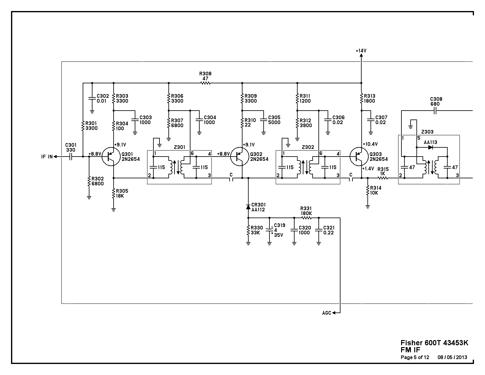
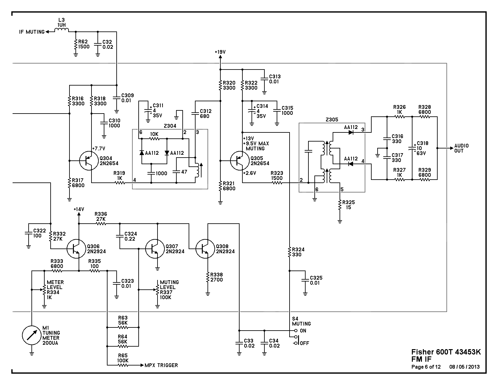
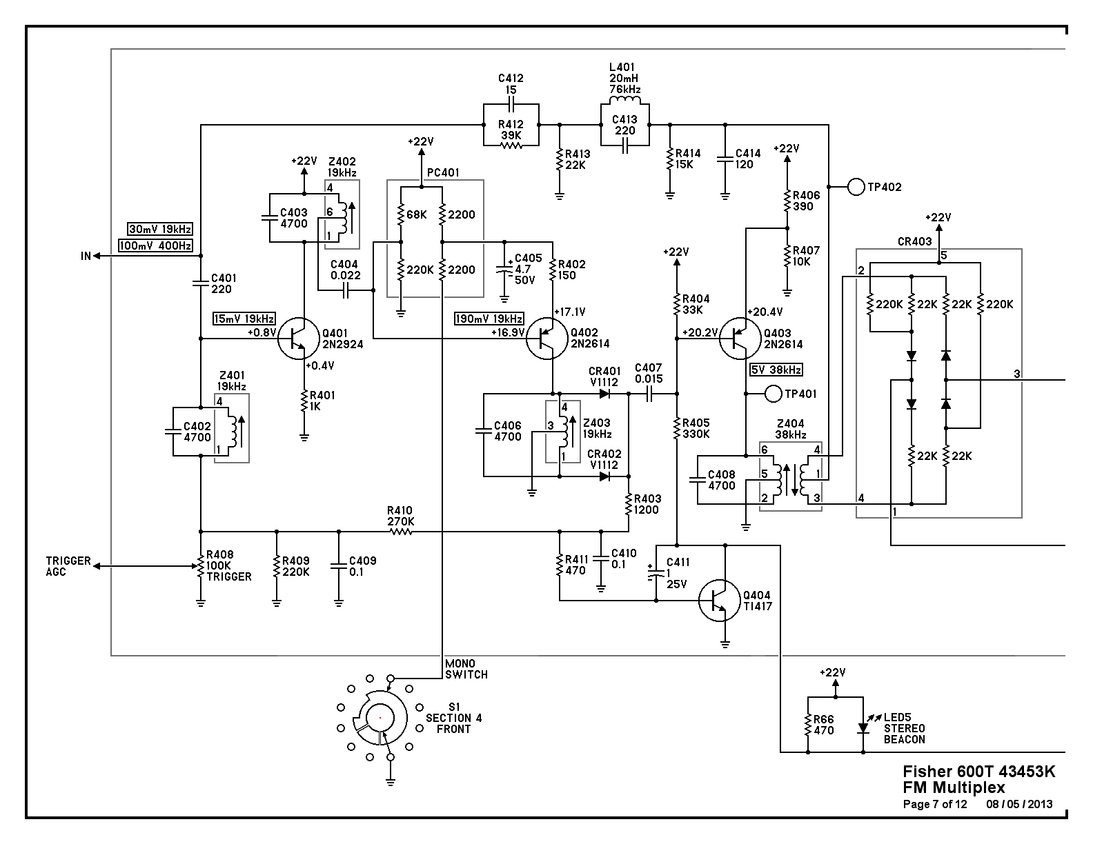
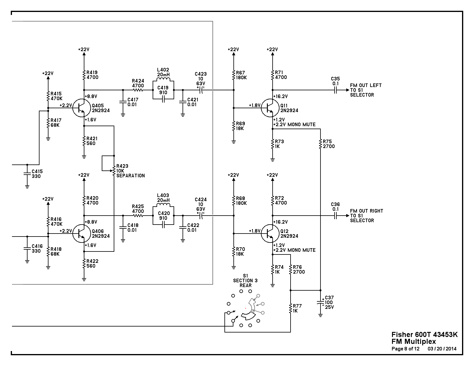
Schematic Diagrams
Since much of the on chassis circuitry was modified, the schematics were redrawn and new designations were assigned. Any correlation to the original
Fisher schematic is coincidence. I also don't really like schematics with circuitry having lines that go to blank boxes representing various circuit
boards, especially in the control preamp where there are many external connections. Design, testing, and troubleshooting usually involves a functional
section rather than a physical section, so it is desirable to have a circuit board and its external components on the same sheet. The schematic was split
into functional sections that will print on a single sheet without rescaling.
The following text will use these conventions: <R25> indicates a designation on the original Fisher schematic. [R25] indicates a designation on the new schematic.
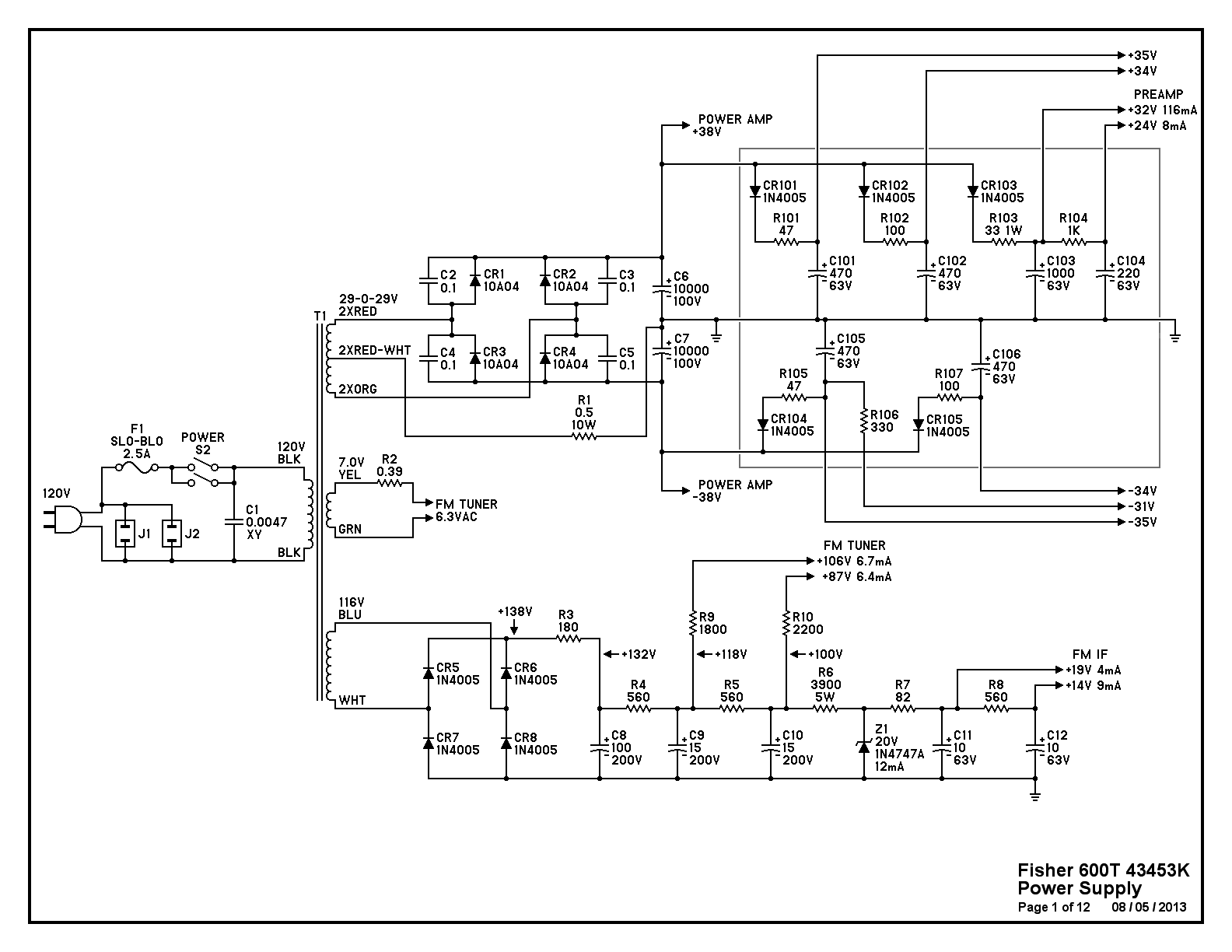
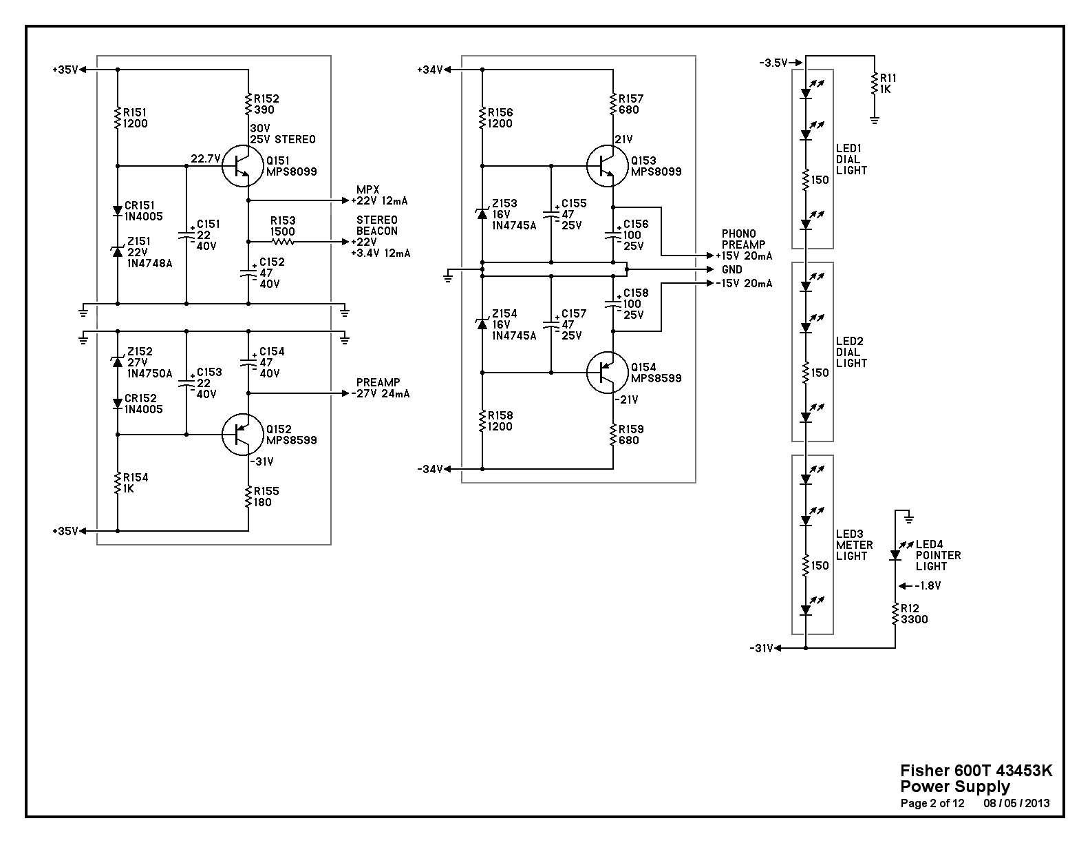
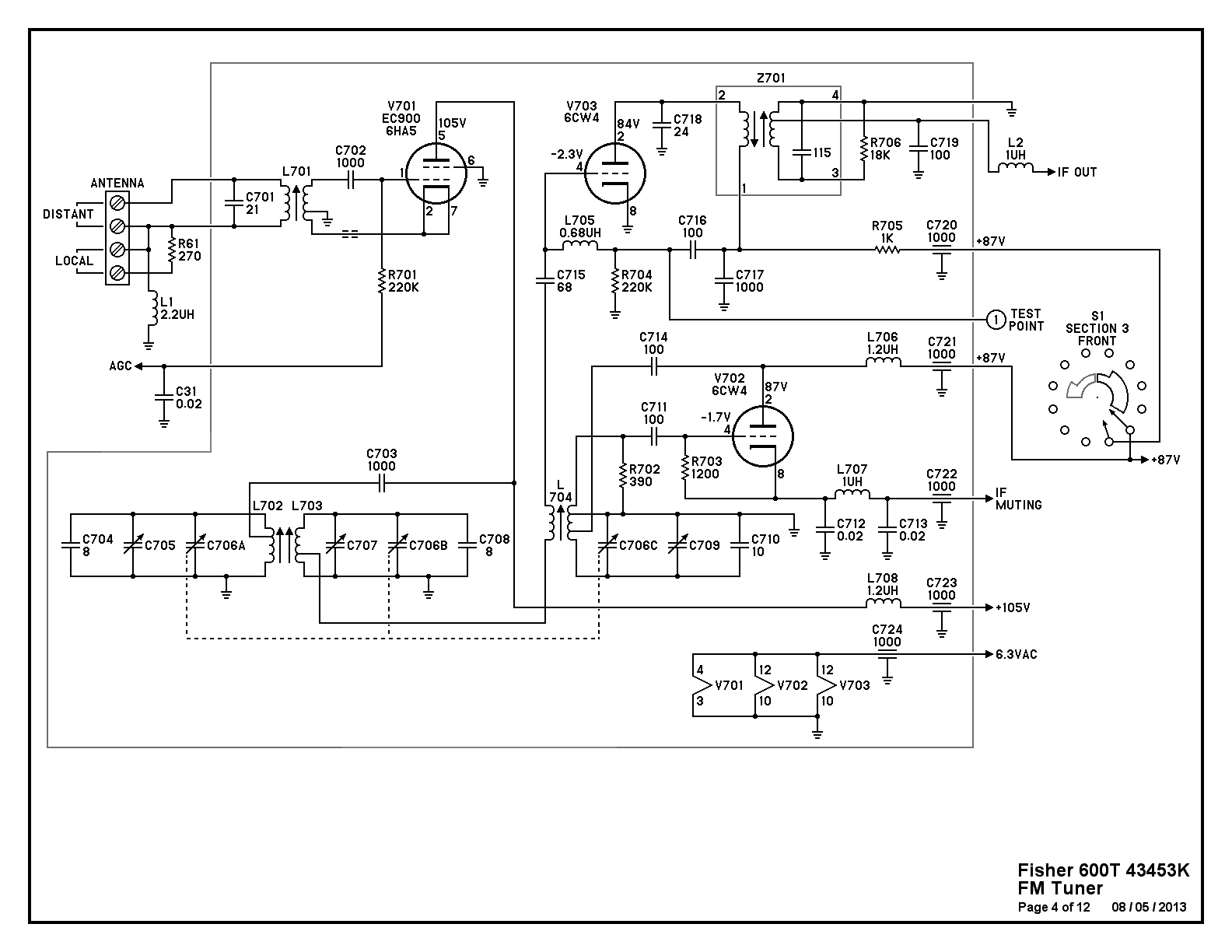
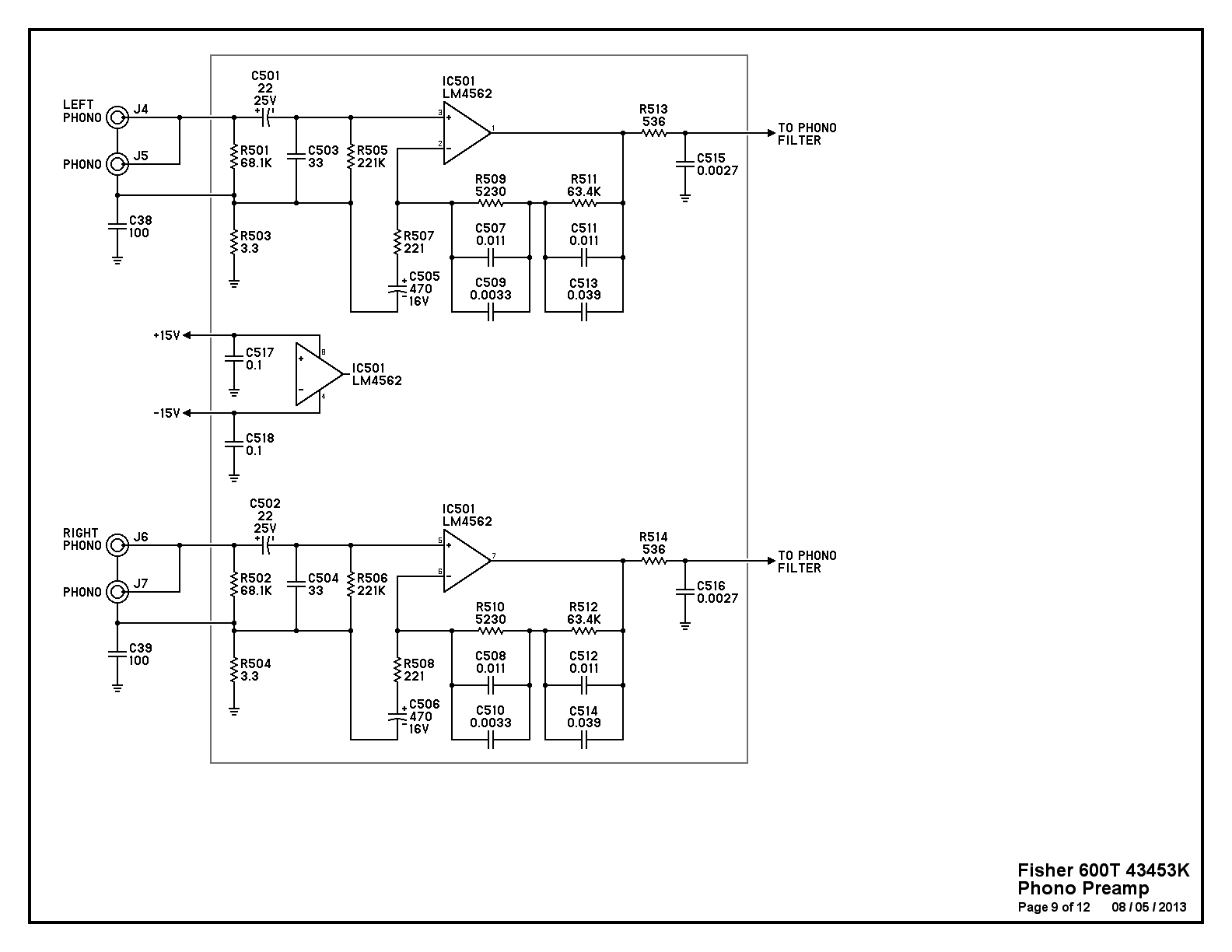
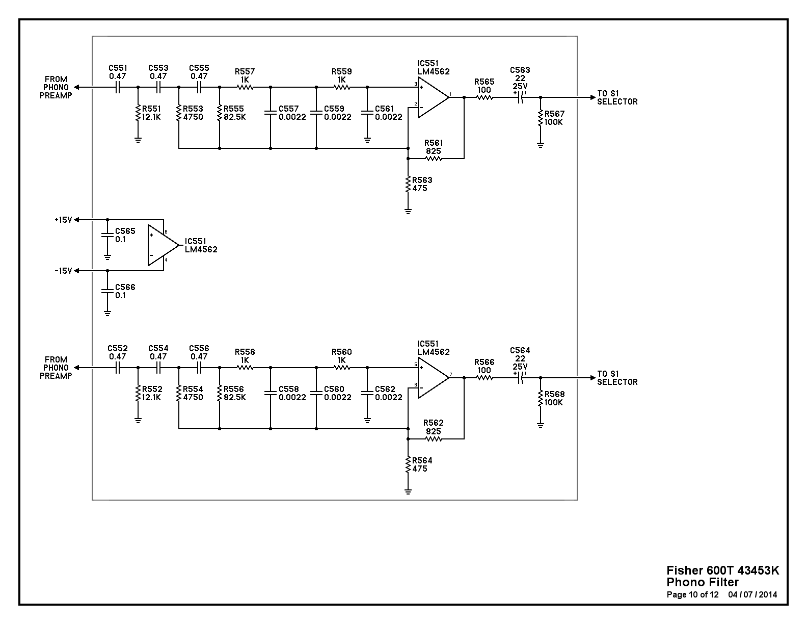
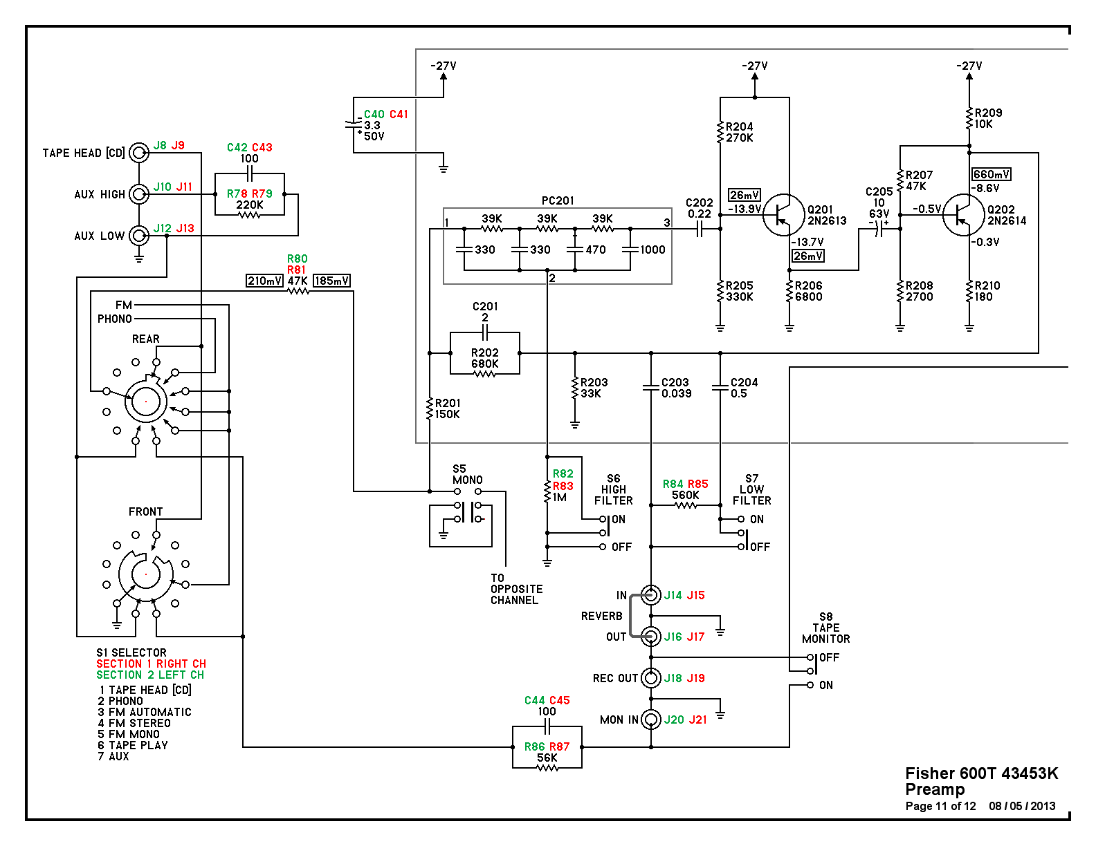
Here are the 12 pages of the revised schematic diagram. Pages 1-2 (power supply) and 9-10 (phono preamp) have significant changes from the original circuit.

Next: Overview Photos
Schematic Diagrams
Since much of the on chassis circuitry was modified, the schematics were redrawn and new designations were assigned. Any correlation to the original
Fisher schematic is coincidence. I also don't really like schematics with circuitry having lines that go to blank boxes representing various circuit
boards, especially in the control preamp where there are many external connections. Design, testing, and troubleshooting usually involves a functional
section rather than a physical section, so it is desirable to have a circuit board and its external components on the same sheet. The schematic was split
into functional sections that will print on a single sheet without rescaling.
The following text will use these conventions: <R25> indicates a designation on the original Fisher schematic. [R25] indicates a designation on the new schematic.
Here are the 12 pages of the revised schematic diagram. Pages 1-2 (power supply) and 9-10 (phono preamp) have significant changes from the original circuit.
Next: Overview Photos
Last edited:
The Hybrid tube amps from consoles you are thinking about are the 49A from the 65' & 66' Custom Electra and the 59A from the 65' Futura and Ambassador. 12ax7 vo
ltage Regulator into 2 6HU8 driver tubes, then xformers to pnp 35144 and 35544 xsistors. Either 4 xsistors(49A) or 8 xsistors for the 59A. EIA watts were 50 and 65w. I'd guess around 15-25 RMS. They do sound pretty nice. I don't play either of mine that much, mainly to save the germanium transistors which are getting to be $30-35 each. But I do have a spare parts chassis.
The President is a TX-1000. My mistake. I've got so many models floating around it makes my trifocals want Lasix surgery.
The GE system that was finally instituted was supposedly superior to the Crosly system. FISHER designed and built mpx decoders for both systems.
Have you ever thought about or tried to change the driver and output transistors over to silicon? I've heard about it but reference's on the net are vague.
Last edited:
fred soop
Super Member
>>>I've got so many models floating around it makes my trifocals want Lasix surgery.
Only up to bifocals here, but multiple reading glasses (computer screen distance is different from printed paper distance) supplemented with Optivisor (especially for some model railroad work) and magnifying glass. Can no longer read much of anything on a DeLorme Atlas without it or the Optivisor. (Proofreading after posting, turns out that OptOvisor is also used but the brand name on mine is OptIvisor.)
>>>Have you ever thought about or tried to change the driver and output transistors over to silicon?
Yes. If everything else was good and I was restoring to original, that would be an option. Converting to NPN would not be a problem either. The output stage could be done with redesign of the bias network. The driver would be a bigger challenge, though the predrivers are already silicon.
With modern transistors, it would no longer be necessary to stack 4 in series to handle the voltage. So, with 8 positions available on the back panel, it would be possible to parallel transistors which would help with beta droop and crossover distortion. However, given the obsolete design overall, a total redesign such as what will be done in 38215G would probably be a better choice.
A while back, the 2N2147 (TR35144 / TR35544) was available on eBay but not at the present. There are some available from Great Britain at £8.00.
I will NOT use NTE "replacements". (note "replacements" in quotes.) Here is the latest NTE horror story: I designed and built 8 power supplies for the Twin City Model Railroad Club, a large O scale operation, open to the public and running 12 hours per day. These power supplies (called "cabs" because they are used to control trains as in locomotive "cab") have to supply up to 8 amps (ancient O scale can be quite current hungry) and withstand long term short circuits. They have been in continuous service since September 29, 1985. Current foldback cannot be used because full current is needed at low output voltage. (Also true of audio amps but not well understood and often improperly implemented.) The design looks a lot like the positive half of a transistor audio power amplifier, good for low frequencies including DC. These use 4 MJ802 power transistors in parallel. DC beta of those transistors is 25 to 100. The technician that has been repairing and maintaining these units since I left has used NTE "replacements" and recently one of the units was sent to me for a repair that stumped him.
The actual problem found was a missing mica washer under a transistor that connected the collector to the case. The secondary side of these units is not connected to the chassis because direction of trains operated on DC is determined by polarity and the floating output can have either side connected to the railroad common as a result.
However, I also measured the NTE "replacements" and discovered that the DC beta is 4. That's not a typo. FOUR !!! To supply 8 amps, the driver would have to supply 2 amps of base current. Ain't gonna happen, at least not for very long.
As for the President TX-1000, the power amplifier circuit looks to be the same as a 700-T. So, where are they getting that 260 watt rating?
fred soop
Super Member
Overview Photos
The camera tends to burn a bit with bright red. The Stereo Beacon and dial pointer lights are pure red and the Stereo Beacon is almost blinding if viewed
directly from the front.
1403
Rear panel. The Tape Head input is now a high level input and will eventually be relabeled, but only on the rear panel. The front panel will not be modified.
1405
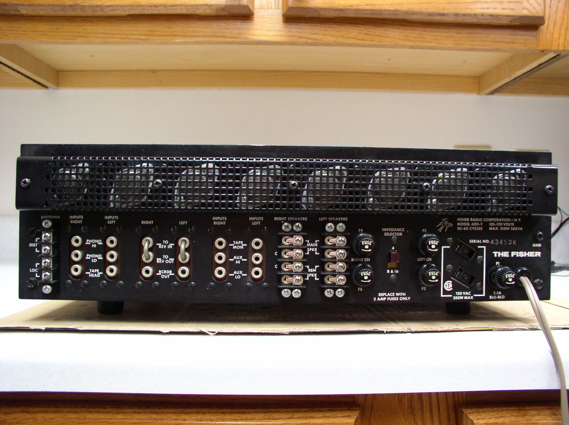
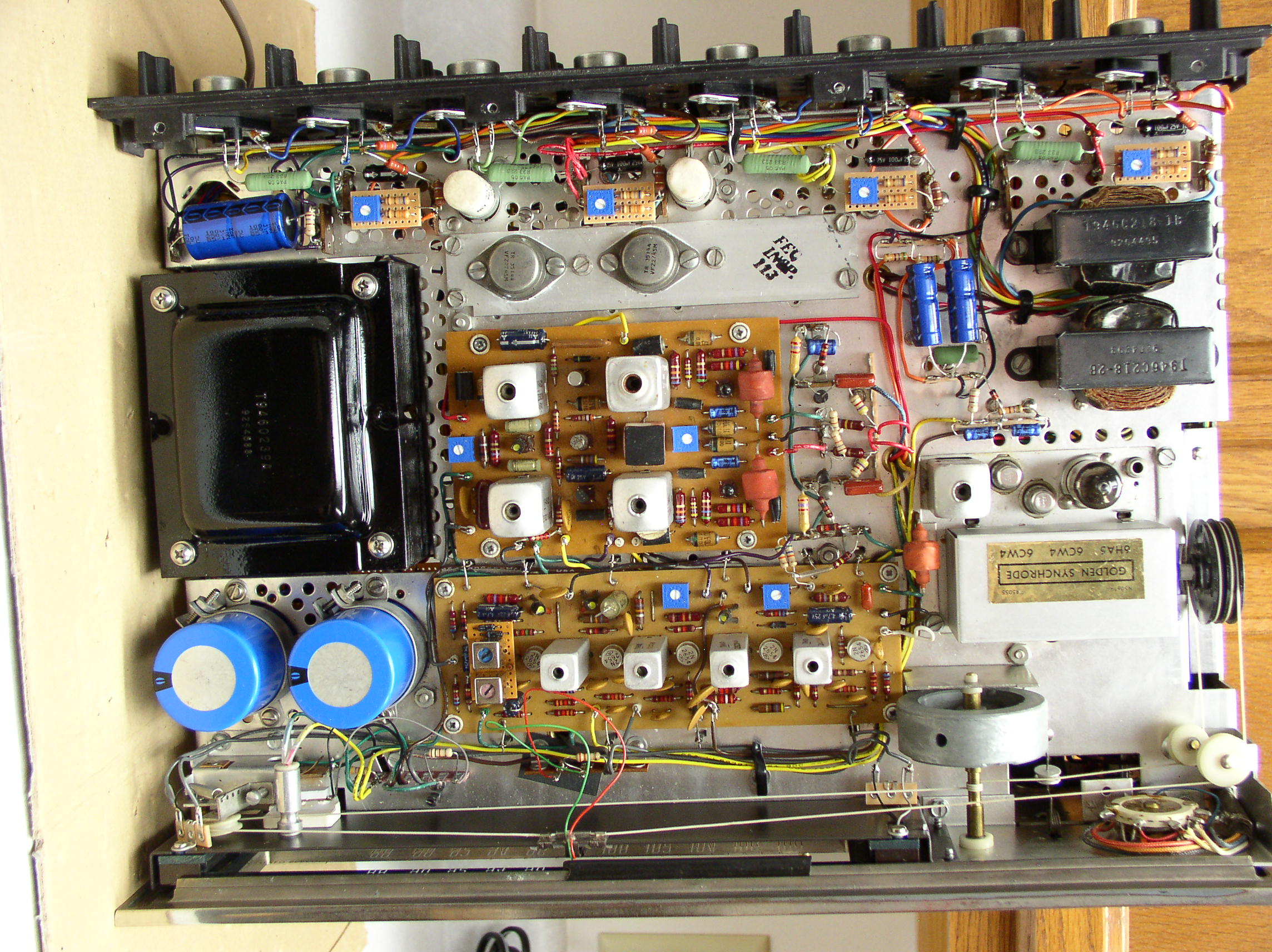
Top view. Some of the details will be discussed later. At the upper left, the can capacitor for the high voltage <C2> has been removed and the first section
<C2A> is replaced with [C8]. The other 2 sections of <C2> are replaced with [C9-C10] located next to the driver transformers. The replacement emitter
resistors along the rear panel [R31 R32 R47 R48] are easily accessed to measure bias voltage. The small pc boards are the modified bias adjustments.
(Transistor version of IBAM?) Note that the rebuilt power amplifier uses new 2 watt resistors that are much smaller than the old resistors. Capacitors today
are also much smaller, allowing for a neater installation.
Between the driver transformers and the FM front end is a regulated supply for the IF amplifier, derived from the front end high voltage supply. At the lower
left, the main filter capacitors <C25 C26> are replaced with new capacitors [C6 C7]. New, better quality, enclosed trimpots were installed on the IF and
Multiplex boards. Dial, meter, and dial pointer lights were replaced with LEDs and the 2 resistors near the front panel are easily accessible if they need to
be changed for brightness.
1407
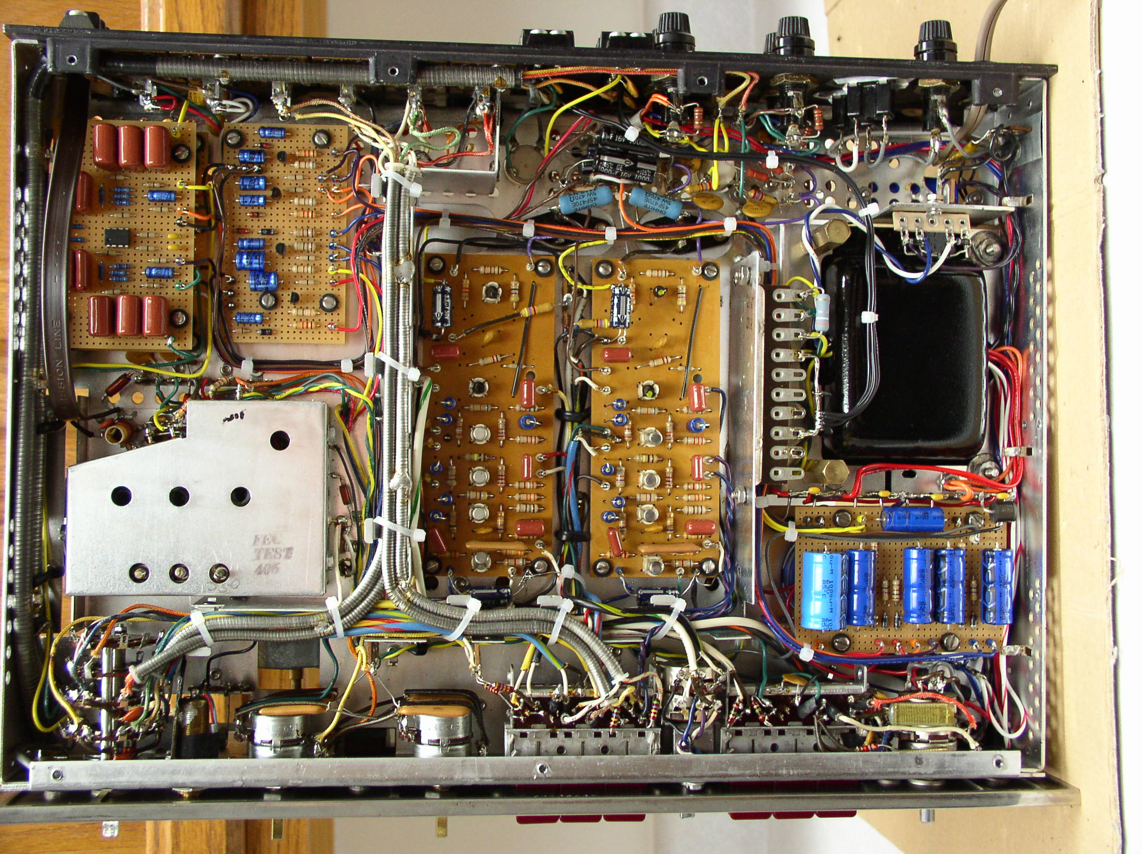
Bottom view. At the upper left is the new phono preamp, subsonic and ultrasonic filter (stacked above the phono preamp), and a board with voltage regulators.
To the right of that is the rewired driver amplifier. At the upper right, removal of the can capacitor <C2> and selenium rectifier <CR5> leaves the space
open for exclusive use by the mains wiring. Just below that is a terminal strip with diodes [CR5 through CR8], replacing selenium rectifier <CR5> for the high
voltage. Below the transformer and mounted over the main filter capacitors is a power supply board with the second level of filtering.
1408
next: Restoration Details
The camera tends to burn a bit with bright red. The Stereo Beacon and dial pointer lights are pure red and the Stereo Beacon is almost blinding if viewed
directly from the front.
1403
Rear panel. The Tape Head input is now a high level input and will eventually be relabeled, but only on the rear panel. The front panel will not be modified.
1405
Top view. Some of the details will be discussed later. At the upper left, the can capacitor for the high voltage <C2> has been removed and the first section
<C2A> is replaced with [C8]. The other 2 sections of <C2> are replaced with [C9-C10] located next to the driver transformers. The replacement emitter
resistors along the rear panel [R31 R32 R47 R48] are easily accessed to measure bias voltage. The small pc boards are the modified bias adjustments.
(Transistor version of IBAM?) Note that the rebuilt power amplifier uses new 2 watt resistors that are much smaller than the old resistors. Capacitors today
are also much smaller, allowing for a neater installation.
Between the driver transformers and the FM front end is a regulated supply for the IF amplifier, derived from the front end high voltage supply. At the lower
left, the main filter capacitors <C25 C26> are replaced with new capacitors [C6 C7]. New, better quality, enclosed trimpots were installed on the IF and
Multiplex boards. Dial, meter, and dial pointer lights were replaced with LEDs and the 2 resistors near the front panel are easily accessible if they need to
be changed for brightness.
1407
Bottom view. At the upper left is the new phono preamp, subsonic and ultrasonic filter (stacked above the phono preamp), and a board with voltage regulators.
To the right of that is the rewired driver amplifier. At the upper right, removal of the can capacitor <C2> and selenium rectifier <CR5> leaves the space
open for exclusive use by the mains wiring. Just below that is a terminal strip with diodes [CR5 through CR8], replacing selenium rectifier <CR5> for the high
voltage. Below the transformer and mounted over the main filter capacitors is a power supply board with the second level of filtering.
1408
next: Restoration Details
fred soop
Super Member
Now, the details that all of you have been patiently waiting for .....
Note: After writing this several weeks ago, it has become apparent that many of you already know many of the details, so some of this may be written below your level.
Power Supply
The power supply should always be considered first because if that isn't working optimally, then analysis of anything else is a waste of time.
If there are any doubts concerning the power amplifier, the 4 fuses on the back panel should be removed before proceeding. In some cases, all loads on the
power supply should be disconnected until all sections of the power supply are functioning properly.
When this equipment was designed and built, the voltage at the wall outlet was approximately 110 volts. Today, it is closer to 120 volts and I have measured
as high as 122 volts at the workbench. This raises all internal voltages. The main supply is shown as +/- 36 volts but measures slightly over +/- 38 volts.
The original main filter capacitors were rated at 40 volts. Since ALL electrolytic capacitors were being replaced, this would no longer be a problem.
The capacitors are almost 50 years old and if they are still good today, they may not be tomorrow. The 6.3 volt supply for the front end tube heaters and the
dial lights measured 7.0 volts. Too high for long term operation.
While my meters all agree on DC voltages, it seems to be difficult to get a consistent AC voltage reading. The 7.0 volts was eventually measured with the
scope and the wave is not a pure sine wave which could explain the meter discrepancy.
Spec sheets for the tubes call for 6.3 volts +/- 10%. The high voltage bridge rectifier <CR5> was a selenium unit. This was replaced with silicon diodes [CR5- CR8],
which actually solves the problem with lower voltage due to the modified transformer winding. Power transformers had already been swapped between units.
Safety
The AC input had a small capacitor <C28 0.01 μf> from one line to chassis and a resistor <R56 820K> from the other line to chassis. It was decided to remove
any connection between line and chassis. A capacitor [C1] that is XY rated was installed across the line. If the original configuration is maintained, the
line to chassis capacitor should be replaced with a modern XY rated capacitor. Digi-Key BC2379-ND, Vishay VY1472M63Y5UQ63V0, at 71 cents is X1Y1 rated, and is
therefore suited for line to line (X) or line to chassis (Y) applications. Mouser has it for a penny less. Most of us should just buy a bag full and be done with it.
The original line cord is non polarized. Even with the line filters lifted from the chassis, there is still the ancient power transformer which has capacitive
coupling between the primary winding and the core. With the unit disconnected from all other equipment, a sensitive digital voltmeter measured 94 volts from
chassis to earth ground. Reversing the plug reduced this to 6 volts. Using a Triplett analog meter, the voltages are reduced to 35 volts and 0 volts, so
there is obviously very little current available. Connection to other equipment will affect these readings. The plug was marked as to which side should go the
the return side (wide blade) of the receptacle to minimize this voltage.
Repeating the test with a 1500 ohm resistor and 0.15 μf capacitor (a recommended standard), measured voltage was under 0.05 volts for any
combination of power on/off or plug orientation. Maximum allowable for safety is 0.35 volts, so this should be safe.
The power switch has been noted as a weak link on vintage Fisher tube equipment. Similar problems have not been reported with the lower current draw
of the transistor receivers but the switched receptacles on the rear panel were rewired to be unswitched and both poles of the power switch wired in parallel
to help prolong the life of the switch. Note that this is a marginal solution because with any set of parallel contacts, one will make / break before the other.
The interlock switch <S3> was removed. On this unit, it appears that the switch was installed but never connected. There was no evidence of the contacts ever
being soldered. As for safety, anyone reading this probably knows what not to touch. I'm sure that all of us have been kicked across the room at some point
early in our careers.
Here is the revised mains wiring with [C1] visible.
1409

next: Secondary side of power supply
Note: After writing this several weeks ago, it has become apparent that many of you already know many of the details, so some of this may be written below your level.
Power Supply
The power supply should always be considered first because if that isn't working optimally, then analysis of anything else is a waste of time.
If there are any doubts concerning the power amplifier, the 4 fuses on the back panel should be removed before proceeding. In some cases, all loads on the
power supply should be disconnected until all sections of the power supply are functioning properly.
When this equipment was designed and built, the voltage at the wall outlet was approximately 110 volts. Today, it is closer to 120 volts and I have measured
as high as 122 volts at the workbench. This raises all internal voltages. The main supply is shown as +/- 36 volts but measures slightly over +/- 38 volts.
The original main filter capacitors were rated at 40 volts. Since ALL electrolytic capacitors were being replaced, this would no longer be a problem.
The capacitors are almost 50 years old and if they are still good today, they may not be tomorrow. The 6.3 volt supply for the front end tube heaters and the
dial lights measured 7.0 volts. Too high for long term operation.
While my meters all agree on DC voltages, it seems to be difficult to get a consistent AC voltage reading. The 7.0 volts was eventually measured with the
scope and the wave is not a pure sine wave which could explain the meter discrepancy.
Spec sheets for the tubes call for 6.3 volts +/- 10%. The high voltage bridge rectifier <CR5> was a selenium unit. This was replaced with silicon diodes [CR5- CR8],
which actually solves the problem with lower voltage due to the modified transformer winding. Power transformers had already been swapped between units.
Safety
The AC input had a small capacitor <C28 0.01 μf> from one line to chassis and a resistor <R56 820K> from the other line to chassis. It was decided to remove
any connection between line and chassis. A capacitor [C1] that is XY rated was installed across the line. If the original configuration is maintained, the
line to chassis capacitor should be replaced with a modern XY rated capacitor. Digi-Key BC2379-ND, Vishay VY1472M63Y5UQ63V0, at 71 cents is X1Y1 rated, and is
therefore suited for line to line (X) or line to chassis (Y) applications. Mouser has it for a penny less. Most of us should just buy a bag full and be done with it.
The original line cord is non polarized. Even with the line filters lifted from the chassis, there is still the ancient power transformer which has capacitive
coupling between the primary winding and the core. With the unit disconnected from all other equipment, a sensitive digital voltmeter measured 94 volts from
chassis to earth ground. Reversing the plug reduced this to 6 volts. Using a Triplett analog meter, the voltages are reduced to 35 volts and 0 volts, so
there is obviously very little current available. Connection to other equipment will affect these readings. The plug was marked as to which side should go the
the return side (wide blade) of the receptacle to minimize this voltage.
Repeating the test with a 1500 ohm resistor and 0.15 μf capacitor (a recommended standard), measured voltage was under 0.05 volts for any
combination of power on/off or plug orientation. Maximum allowable for safety is 0.35 volts, so this should be safe.
The power switch has been noted as a weak link on vintage Fisher tube equipment. Similar problems have not been reported with the lower current draw
of the transistor receivers but the switched receptacles on the rear panel were rewired to be unswitched and both poles of the power switch wired in parallel
to help prolong the life of the switch. Note that this is a marginal solution because with any set of parallel contacts, one will make / break before the other.
The interlock switch <S3> was removed. On this unit, it appears that the switch was installed but never connected. There was no evidence of the contacts ever
being soldered. As for safety, anyone reading this probably knows what not to touch. I'm sure that all of us have been kicked across the room at some point
early in our careers.
Here is the revised mains wiring with [C1] visible.
1409
next: Secondary side of power supply
fred soop
Super Member
Main DC Suppy
Changes described here are on pages 1 and 2 of the revised schematic, shown earlier.
As mentioned earlier, the main supply is +/- 38 volts. The 3000 μf main filter capacitors <C25 C26> were replaced with 10,000 μf, 100 volt units [C6 C7].
These are Digi-Key p/n 338-2127-ND, CDE 382LX103M100N062, at $12.95 each. They were selected in part due to being the correct diameter to fit in the existing
clamps with minor bending. They are not as tall as the originals, so the clamps were drilled out and remounted above the chassis so the additional space gained
underneath can be put to use later.
Top view.
1410

Bottom view also showing the standoffs for the board with additional filters.
1414
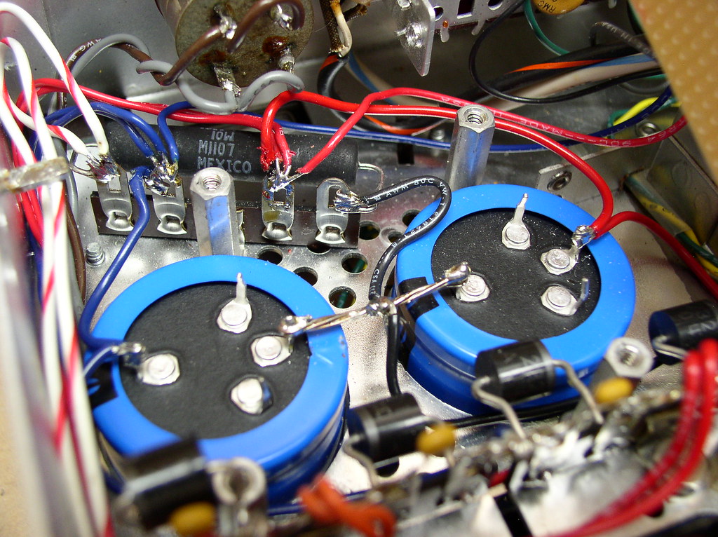
The original diode rectifiers <CR1 through CR4> were ok but, being house numbers, specifications are not available. The larger filter capacitors will
have a greater inrush, the diodes are not extremely expensive, so they were replaced [CR1 through CR4] with Digi-Key p/n 10A04-TDICT-ND, DI 10A04T, at 74 cents each.
This photo shows the high voltage diodes [CR5 - CR8] to the right of the transformer. The terminal strip above the transformer is the ground
distribution. There are extra terminals as running design changes were made during the restoration and drilling holes for mounting different terminal
strips is risky once rewiring starts due to small metal particles being scattered. The 3.9 ohm resistor [R2] is to reduce the 7.0 volt heater voltage
to the proper 6.3 volts.
1411

Power for the preamp and multiplex stages is derived from the +/- 38 volt supply. The regulators <Q11, Q12 and associated circuitry> only hold voltage at
a constant value relative to the main supply. With one exception <ZR1 feeding the phono preamp>, there are no zener diodes to determine what that value will
be, or to hold a constant voltage when the main supply sags during high power output. These regulators were removed and redesigned with improved regulators.
Additionally, +/- 15 volts is needed for the new phono preamp to be discussed later.
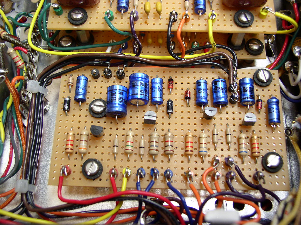
This circuit board contains the second level of filtering before scattering power wires to the far corners of the unit. It is mounted on standoffs above
(below) the main filter capacitors with [C101 C102] (new) [C103 C104] (replacing <C22 C23>) [C105] (replacing <C24 and C27>) and [C106] (new). Note
the color coded test point terminals applied to all the circuit boards. Diodes were added at the input to these filters to prevent voltage sag due to
delivering short bursts of high power from discharging the secondary filter capacitors.
1415
Underside of the same board. It looks like some redundancy on the lower edge with the black wires, but this is done to keep the various ground connections
in the proper order. The single band "resistors" are zero ohms, or jumpers with a resistor body.
1416

Regulators on the board located next to the phono preamp. Note that the mounting screws are not in an exact rectangular pattern. This was done to use
existing chassis holes and avoid excess drilling. At the left is [Q151], the +22 volt multiplex regulator, [Q152 Q153], the +/- 15 volt regulators for the
phono preamp, and [Q154], the -27 volt regulator for the control preamp.
1417
The high voltage supply had the selenium bridge rectifier <CR5> replaced with 1N4005 diodes [CR5 through CR8]. The 3 section can capacitor <C2> was removed
and replaced with 3 individual capacitors [C8 C9 C10]. That supply also provides the +19 and +14 volts for the IF circuit board in addition to the high
voltages for the front end. The +19 and +14 voltages will vary depending on current draw of the front end tubes and will rise during warm up before the
tubes draw plate current. This part of the power supply was modified with a zener diode [Z1] to hold the IF voltage constant.
Since the high voltage / IF supply has numerous resistors and taps, there is only so much calculation and simulation that can be done before building. The
circuit was set up on a breadboard and wired to the various stages so that measurements could be taken and resistor values adjusted.
Photo of [C8] and the hole where <C2> was removed.
1412

Photo of [C9 C10] replacing <C2B C2C>. The +19 and +14 volt regulators for the IF board are out of focus at the upper right.
1413

As mentioned earlier, the 6.3 volt supply measures 7.0 volts. The dial lamps (difficult to find replacements) and the somewhat obnoxious meter lamp were
removed and replaced with LEDs. This, in addition to the higher line voltage, reduces the load on the 6.3 volt supply. A resistor [R2] of 0.39 ohms, 1/2
watt, was added to bring this supply down to a safe level for the tube heaters.
next: Power Amplifier
Changes described here are on pages 1 and 2 of the revised schematic, shown earlier.
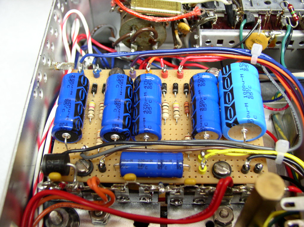
As mentioned earlier, the main supply is +/- 38 volts. The 3000 μf main filter capacitors <C25 C26> were replaced with 10,000 μf, 100 volt units [C6 C7].
These are Digi-Key p/n 338-2127-ND, CDE 382LX103M100N062, at $12.95 each. They were selected in part due to being the correct diameter to fit in the existing
clamps with minor bending. They are not as tall as the originals, so the clamps were drilled out and remounted above the chassis so the additional space gained
underneath can be put to use later.
Top view.
1410
Bottom view also showing the standoffs for the board with additional filters.
1414
The original diode rectifiers <CR1 through CR4> were ok but, being house numbers, specifications are not available. The larger filter capacitors will
have a greater inrush, the diodes are not extremely expensive, so they were replaced [CR1 through CR4] with Digi-Key p/n 10A04-TDICT-ND, DI 10A04T, at 74 cents each.
This photo shows the high voltage diodes [CR5 - CR8] to the right of the transformer. The terminal strip above the transformer is the ground
distribution. There are extra terminals as running design changes were made during the restoration and drilling holes for mounting different terminal
strips is risky once rewiring starts due to small metal particles being scattered. The 3.9 ohm resistor [R2] is to reduce the 7.0 volt heater voltage
to the proper 6.3 volts.
1411
Power for the preamp and multiplex stages is derived from the +/- 38 volt supply. The regulators <Q11, Q12 and associated circuitry> only hold voltage at
a constant value relative to the main supply. With one exception <ZR1 feeding the phono preamp>, there are no zener diodes to determine what that value will
be, or to hold a constant voltage when the main supply sags during high power output. These regulators were removed and redesigned with improved regulators.
Additionally, +/- 15 volts is needed for the new phono preamp to be discussed later.
This circuit board contains the second level of filtering before scattering power wires to the far corners of the unit. It is mounted on standoffs above
(below) the main filter capacitors with [C101 C102] (new) [C103 C104] (replacing <C22 C23>) [C105] (replacing <C24 and C27>) and [C106] (new). Note
the color coded test point terminals applied to all the circuit boards. Diodes were added at the input to these filters to prevent voltage sag due to
delivering short bursts of high power from discharging the secondary filter capacitors.
1415
Underside of the same board. It looks like some redundancy on the lower edge with the black wires, but this is done to keep the various ground connections
in the proper order. The single band "resistors" are zero ohms, or jumpers with a resistor body.
1416
Regulators on the board located next to the phono preamp. Note that the mounting screws are not in an exact rectangular pattern. This was done to use
existing chassis holes and avoid excess drilling. At the left is [Q151], the +22 volt multiplex regulator, [Q152 Q153], the +/- 15 volt regulators for the
phono preamp, and [Q154], the -27 volt regulator for the control preamp.
1417
The high voltage supply had the selenium bridge rectifier <CR5> replaced with 1N4005 diodes [CR5 through CR8]. The 3 section can capacitor <C2> was removed
and replaced with 3 individual capacitors [C8 C9 C10]. That supply also provides the +19 and +14 volts for the IF circuit board in addition to the high
voltages for the front end. The +19 and +14 voltages will vary depending on current draw of the front end tubes and will rise during warm up before the
tubes draw plate current. This part of the power supply was modified with a zener diode [Z1] to hold the IF voltage constant.
Since the high voltage / IF supply has numerous resistors and taps, there is only so much calculation and simulation that can be done before building. The
circuit was set up on a breadboard and wired to the various stages so that measurements could be taken and resistor values adjusted.
Photo of [C8] and the hole where <C2> was removed.
1412
Photo of [C9 C10] replacing <C2B C2C>. The +19 and +14 volt regulators for the IF board are out of focus at the upper right.
1413
As mentioned earlier, the 6.3 volt supply measures 7.0 volts. The dial lamps (difficult to find replacements) and the somewhat obnoxious meter lamp were
removed and replaced with LEDs. This, in addition to the higher line voltage, reduces the load on the 6.3 volt supply. A resistor [R2] of 0.39 ohms, 1/2
watt, was added to bring this supply down to a safe level for the tube heaters.
next: Power Amplifier
fred soop
Super Member
Power Amplifier
Changes described here can be seen on page 3 of the revised schematic, published earlier.
This unit is from the 5th version, s/n 41001 and up, and the bias adjustment pots were replaced with free standing diodes starting with the 4th version, s/n 39000 - 41000.
The adjustment pots were open wirewound units subject to getting dirty and intermittent. Likely the cause of some of the early failures. There were
resistors in parallel but they may or may not protect against open wipers on the pots. Bias with the diode modification is dependent on component
tolerances. One channel appeared to be ok but the other channel was at about half the specified bias. Both channels had a small DC output at the speaker terminals.
Service manuals for earlier versions with the bias pots specified setting the bias using an intermodulation distortion analyzer. Something we all have
sitting right next to the voltmeter. Oh, you don't have one either? What a coincidence. Guess we'll have to improvise. After the change to non adjustable
bias, this was changed and the schematic indicates that there should be 19 mV across the 0.33 ohm emitter resistors <R97 through R100>. Be careful as this
does not directly represent emitter current. These resistors are also carrying part of the current for the bias network. My revised circuit has the emitter
resistors [R31 R32 R47 R48] handling only the transistor emitter current. I determined that the idle current should be approximately 30 mA. The replacement
emitter resistors are 1% tolerance. While this isn't necessary for performance of the circuit, it does allow for greater accuracy in bias current measurements.
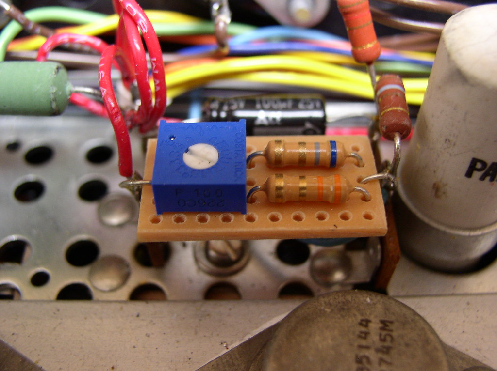
I determined that the best way to correct this circuit was a return to the bias adjustments, but make them reliable. (transistor version of IBAM?) The diodes
<CR6 through CR9> of the later circuit were not attached to the heat sink so none of the versions ever had any direct thermal feedback. My revised bias
circuit uses a 10 ohm Bourns trimpot [R27 R28 R43 R44] in series with a 3.3 ohm resistor [R25 R26 R41 R42]. That combination is in parallel with a 6.8 ohm
resistor [R29 R30 R45 R46], so the entire combination can only be adjusted between 2.5 and 4.5 ohms and even if the wiper on the pot were to lose contact,
it can't go over 4.5 ohms, raising the bias to 60 mA, double the specified value, and probably not harmful. That would be 1.14 watts per transistor at
idle. The bias circuit was determined first by calculation, then by a lot of testing. The bias can be adjusted from half to double the specified value. The
pot is a sealed unit, so should be reliable over the long term.
Bias adjustment will be described later. There is still a test for the 4th and 5th revisions using the IM distortion analyzer and what the results should be
but nothing stating what to do if the distortion is out of spec.
1424
There were a couple of wiring errors, apparently from the factory, because the solder joints appeared to have never been disturbed. The 5th revision, s/n 41001
and up, has an error in the schematic diagram. There are 2.2 ohm resistors <R112 through R115> added to the collector circuits of output transistors <Q1
Q3 Q5 Q7> and the bias resistors <R73 through R76 and R83 through R86> are shown connected to the top side of these resistors. A small resistor in a
collector circuit with nothing connected between that resistor and the collector will do nothing. The unit actually had the bias resistor connection
made to the lower end of these resistors.
There are 4 electrolytic capacitors <C39 through C42> that are buried under a lot of resistors that make up the bias network. Since I was doing some
redesign, resistors are cheap, and they were in the way, I ended up completely stripping the power amplifier and rewiring. One advantage of this is that
todays 2 watt resistors are about the size of yesterdays 1/2 watt units so the circuit looks much neater after rebuilding. Before stripping, ALL wires on the
driver transformers <T2 T3> must be carefully labeled. If they ever got connected with the upper and lower drives in phase, the first signal applied
would turn on all 4 transistors and blow the entire thing sky high.
All power transistors were removed, cleaned, the heat sink cleaned, and transistors remounted with new insulating washers and fresh thermal grease.
After this, all were checked for possible case to chassis shorts. Soldering to the transistor sockets was done with the transistors removed to reduce the
possibility of heat damage. Some minimal rework was done later with the transistors installed.
1406

Since the actual output stage is isolated via the driver transformer, it can be tested independently of everything else. An external power supply was used, one
that I built many years ago. It is a dual supply with voltage adjusted by a variac on the AC line side. This was connected to the output stage (don't
forget the ground connection) and voltage brought up to approximately +/- 10 volts. All voltages were measured and found to be at acceptable levels. The
process was repeated for increasing voltage until the amplifier was up to the full +/- 38 volt supply.
Adjusting Bias
A voltmeter was connected across one of the emitter resistors and the associated trimpot adjusted for 10 mV, corresponding to 30 mA of emitter
current. The other trimpot in that channel was then turned to approximately the same physical position because the adjustments for the upper and lower
transistor pairs interact and this would get the adjustments closer to start. Then the voltage at the other emitter resistor was checked. Adjustments were
repeated several times until correct. Next, the DC output offset voltage should be measured. If it is positive, then the upper transistor pair needs slightly
less bias and the lower slightly more. If the voltage is negative, then the opposite. This is a very small adjustment. Before you think this is backwards,
remember that we are dealing with PNP transistors and the upper pair leads to the negative supply.
Bias was actually set approximately at first, then the amplifier was allowed to cook at about 10 watts, then the bias set with the output warmed up. Why 10
watts rather than full power? In normal operation, the average power delivered is going to be low enough such that peak signal levels are still within power
limits. Probably much lower than even 10 watts.
After several months of use, it was noted that the bias adjustments needed trimming. The bias had drifted up to around 12 mV (36 mA idle current).
Output Transistors
As mentioned earlier, the output transistors are house numbered versions of either 2N2147 or 2N2148. They are the same except the 2N2147 has slightly
higher voltage ratings. Be careful of replacement cross references. One of these 2 (don't remember which) crosses to a small signal transistor and more
recently, I've heard that the NTE cross reference is also incorrect for at least one of them. Actually, I'd probably redesign and rebuild before replacing
expensive transistors in this circuit. The TX-300 and early versions of the 600-T and some consoles show 2 different transistor numbers for the 4
transistors, but they were changed to the same part in later versions of the 600-T. I don't think it matters as long as the beta of the 4 transistors within
a channel are close. Since the power amplifier is independent (due to the driver transformers) it would be possible to redesign using more rugged and
readily available NPN (or PNP) silicon devices but I'd just design a completely new circuit first. Good as the present circuit is, unfortunately, it's simply
obsolete. 38215G will eventually have a redesigned circuit.
I should probably add catch diodes and a Zobel network. I'm guessing that the problems solved by those were not discovered in the early transistor era.
next: Driver and Control Preamp
Changes described here can be seen on page 3 of the revised schematic, published earlier.
This unit is from the 5th version, s/n 41001 and up, and the bias adjustment pots were replaced with free standing diodes starting with the 4th version, s/n 39000 - 41000.
The adjustment pots were open wirewound units subject to getting dirty and intermittent. Likely the cause of some of the early failures. There were
resistors in parallel but they may or may not protect against open wipers on the pots. Bias with the diode modification is dependent on component
tolerances. One channel appeared to be ok but the other channel was at about half the specified bias. Both channels had a small DC output at the speaker terminals.
Service manuals for earlier versions with the bias pots specified setting the bias using an intermodulation distortion analyzer. Something we all have
sitting right next to the voltmeter. Oh, you don't have one either? What a coincidence. Guess we'll have to improvise. After the change to non adjustable
bias, this was changed and the schematic indicates that there should be 19 mV across the 0.33 ohm emitter resistors <R97 through R100>. Be careful as this
does not directly represent emitter current. These resistors are also carrying part of the current for the bias network. My revised circuit has the emitter
resistors [R31 R32 R47 R48] handling only the transistor emitter current. I determined that the idle current should be approximately 30 mA. The replacement
emitter resistors are 1% tolerance. While this isn't necessary for performance of the circuit, it does allow for greater accuracy in bias current measurements.
I determined that the best way to correct this circuit was a return to the bias adjustments, but make them reliable. (transistor version of IBAM?) The diodes
<CR6 through CR9> of the later circuit were not attached to the heat sink so none of the versions ever had any direct thermal feedback. My revised bias
circuit uses a 10 ohm Bourns trimpot [R27 R28 R43 R44] in series with a 3.3 ohm resistor [R25 R26 R41 R42]. That combination is in parallel with a 6.8 ohm
resistor [R29 R30 R45 R46], so the entire combination can only be adjusted between 2.5 and 4.5 ohms and even if the wiper on the pot were to lose contact,
it can't go over 4.5 ohms, raising the bias to 60 mA, double the specified value, and probably not harmful. That would be 1.14 watts per transistor at
idle. The bias circuit was determined first by calculation, then by a lot of testing. The bias can be adjusted from half to double the specified value. The
pot is a sealed unit, so should be reliable over the long term.
Bias adjustment will be described later. There is still a test for the 4th and 5th revisions using the IM distortion analyzer and what the results should be
but nothing stating what to do if the distortion is out of spec.
1424
There were a couple of wiring errors, apparently from the factory, because the solder joints appeared to have never been disturbed. The 5th revision, s/n 41001
and up, has an error in the schematic diagram. There are 2.2 ohm resistors <R112 through R115> added to the collector circuits of output transistors <Q1
Q3 Q5 Q7> and the bias resistors <R73 through R76 and R83 through R86> are shown connected to the top side of these resistors. A small resistor in a
collector circuit with nothing connected between that resistor and the collector will do nothing. The unit actually had the bias resistor connection
made to the lower end of these resistors.
There are 4 electrolytic capacitors <C39 through C42> that are buried under a lot of resistors that make up the bias network. Since I was doing some
redesign, resistors are cheap, and they were in the way, I ended up completely stripping the power amplifier and rewiring. One advantage of this is that
todays 2 watt resistors are about the size of yesterdays 1/2 watt units so the circuit looks much neater after rebuilding. Before stripping, ALL wires on the
driver transformers <T2 T3> must be carefully labeled. If they ever got connected with the upper and lower drives in phase, the first signal applied
would turn on all 4 transistors and blow the entire thing sky high.
All power transistors were removed, cleaned, the heat sink cleaned, and transistors remounted with new insulating washers and fresh thermal grease.
After this, all were checked for possible case to chassis shorts. Soldering to the transistor sockets was done with the transistors removed to reduce the
possibility of heat damage. Some minimal rework was done later with the transistors installed.
1406
Since the actual output stage is isolated via the driver transformer, it can be tested independently of everything else. An external power supply was used, one
that I built many years ago. It is a dual supply with voltage adjusted by a variac on the AC line side. This was connected to the output stage (don't
forget the ground connection) and voltage brought up to approximately +/- 10 volts. All voltages were measured and found to be at acceptable levels. The
process was repeated for increasing voltage until the amplifier was up to the full +/- 38 volt supply.
Adjusting Bias
A voltmeter was connected across one of the emitter resistors and the associated trimpot adjusted for 10 mV, corresponding to 30 mA of emitter
current. The other trimpot in that channel was then turned to approximately the same physical position because the adjustments for the upper and lower
transistor pairs interact and this would get the adjustments closer to start. Then the voltage at the other emitter resistor was checked. Adjustments were
repeated several times until correct. Next, the DC output offset voltage should be measured. If it is positive, then the upper transistor pair needs slightly
less bias and the lower slightly more. If the voltage is negative, then the opposite. This is a very small adjustment. Before you think this is backwards,
remember that we are dealing with PNP transistors and the upper pair leads to the negative supply.
Bias was actually set approximately at first, then the amplifier was allowed to cook at about 10 watts, then the bias set with the output warmed up. Why 10
watts rather than full power? In normal operation, the average power delivered is going to be low enough such that peak signal levels are still within power
limits. Probably much lower than even 10 watts.
After several months of use, it was noted that the bias adjustments needed trimming. The bias had drifted up to around 12 mV (36 mA idle current).
Output Transistors
As mentioned earlier, the output transistors are house numbered versions of either 2N2147 or 2N2148. They are the same except the 2N2147 has slightly
higher voltage ratings. Be careful of replacement cross references. One of these 2 (don't remember which) crosses to a small signal transistor and more
recently, I've heard that the NTE cross reference is also incorrect for at least one of them. Actually, I'd probably redesign and rebuild before replacing
expensive transistors in this circuit. The TX-300 and early versions of the 600-T and some consoles show 2 different transistor numbers for the 4
transistors, but they were changed to the same part in later versions of the 600-T. I don't think it matters as long as the beta of the 4 transistors within
a channel are close. Since the power amplifier is independent (due to the driver transformers) it would be possible to redesign using more rugged and
readily available NPN (or PNP) silicon devices but I'd just design a completely new circuit first. Good as the present circuit is, unfortunately, it's simply
obsolete. 38215G will eventually have a redesigned circuit.
I should probably add catch diodes and a Zobel network. I'm guessing that the problems solved by those were not discovered in the early transistor era.
next: Driver and Control Preamp
fred soop
Super Member
Why do you guys post such large pictures?
Not everyone has 2 acres of screen real estate . :banghead
18 years ago, I was writing software applications where the display had to be limited to 800 x 600, but that was 18 years ago. The standard for the last half decade has been 1920 x 1080, same as HDTV. Of 11 monitor selections on the Hewlett Packard web site, only 2 are smaller than 1920 x 1080 and those are 1600 x 900.
As of 2012, 18% of web users were using 1024 x 768 and 19% were using 1366 x 768. 13% were using 1280 x 800. That's 50%. Only 3% were still using displays that could not accommodate 1024 x 766 photos without scrolling.
Above photos are mostly 1024 x 766. One in the last post is 1600 x 1197 but the relevant vertical portion is about 475, so would still fit on a 1920 x 1080 display. Scroll bars are preferable to mosaic photos.
iPhones, of course, are a different issue altogether.
The record companies do not continue to produce 78 rpm records just for those that refuse to upgrade to a 33 rpm turntable.