• The move to the new server is done. There are some software and database maintenance updates in process. This has us passing the hat around to help out. We appreciate any donations. Seriously, even a dollar helps. The payment page may be found here - https://www.audiokarma.org/support.html

2325 PH01 buffer amplifier - one channel out

runningdog

AK Subscriber
Subscriber
This 2325 PH01 buffer amplifier is not passing the signal through one channel. I've found where the signal stops (at HH01), and that the voltage at its base is well below what it should be.

HH01 and HH03 should both have 14.2V at their bases. HH01 has only 1.1v. This simplified schematic is highlighted to show where the voltages are correct (yellow) and where not (red):
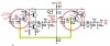
2325 PH01 left channel schematic redrawn by TC.jpg

The current does not seem to be passing through RH07 to HH01, as it does through RH09 to HH03. RH07 tested good, and replacing it made no difference.

Why is the voltage at the base of HH01 only 1.1v?

Thanks in advance.
 
Register to hide this ad
It looks like there is too much current flowing actually and it has to going somewhere! If this has been untouched until you got it a solder short is unlikely... unless someone else has worked on it! If CH01 were shorted that may do it but unlikely. If HH01's emitter is a bit lower than the base, say 0.3 to 0.6 volts it's probably okay. Maybe HH11 is open on HH09's base so it is turning on harder and current flow through it's 75 ohm emitter resistor is lower, messing up HH01?

Anyway, as I've had a number of these boards go bad on me, some after a recap and during burn in, I always replace all transistors and those blob diodes as well. Here are the subs I use:

2SA720 -> KSA1013
2SC1345 -> KSC1845
2SC1318 -> KSC2383

Oh, and watch out for the wrong polarity silkscreen on the local filter cap, the minus side is closer to an edge of the board.

Happy Hunting!
 
Thank you Randy! I'm the first person to work on the board and I have been holding off recapping it until I resolve this issue.

The first time I put in CH13 backwards was before I knew about the silkscreens being wrong. The second time I put in a CH13 backwards was on a board that was marked correctly but I assumed it was wrong. Heh. Now I know...negative towards the edge regardless of marking.
 
It looks like there is too much current flowing actually and it has to going somewhere!

This got me looking for where the current was coming from. I asked myself what would Tom do? He'd get out his Huntron Tracker and look for failed components in circuit. So I did. I thought HH05 was a likely candidate, and on the first touch of the probes I found C and E shorted. Pulled and replaced as you recommended. Now HH01 and HH05 are showing correct voltage.

Now the signal is getting clear to HH09, but not quite making it the to the jumper. The schematic shows it passes through CH05 on the way, one of the four 4.7uF/35v electrolytics. I pulled it out, and what do you know? It was open. Replaced it. And the buffer amplifier is working again. WhooHoo!

This is consistent with the first thing I noticed when I examined the board. There was smoky residue on CH05.

I'll do as Randy does and replace the rest of the semiconductors to finish rebuilding the board.
 
Nice work! Sometimes having two bad components in a faulty signal path makes the diagnosis four times more difficult.
 
I'll do as Randy does and replace the rest of the semiconductors to finish rebuilding the board.

Well, I did not replace all the transistors. And after about 100 hours of play the buffer amplifier failed again, in the other channel. It seems like a cascading failure, so this time I replaced every semiconductor including the ones I replaced before. The resistor at RH28 showed overheating so I replaced it too.

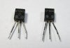
The 2SC1345 transistors at HH03 and HH04 had blackened leads. I've read this indicates a failing component? Or were some leads black to begin with?

2SC1845 with blackened leads.JPG
 
I have never seen a new transistor having black leads when I was a pup tech in 1979. I believe that the leads were silver plated instead of tin or tin/lead. So the black is tarnish. One theory, which makes sense, is that the epoxy can shrink or crack with years of heating and cooling. Then the tarnish can continue on up to the actual semiconductor "dice" and corrupt it. This board is the only one I routinely just get out the shotgun and blast away!
 
Thanks for your answers and tips. I'm so reluctant to shotgun semiconductors although there are notable restorers that do it routinely. And out of maybe fifty 2325 rebuilds this is the only buffer amplifier failure I've seen. On this board I normally just replace the electrolytic caps and the HH11 varistor. But...from now on I'll do all the transistors on this board.

Why is there a buffer amplifier on the 2325? The SM states "all signals are converted to low output impedance by the buffer amplifier". I did notice that the amplitude of the signals do not change going through this board.
 
Back
Top Bottom