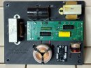
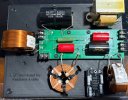
I’ve been working on a modern two-piece layout for the ALK Universal crossover. The design combines a centrally mounted printed circuit board for the smaller capacitors, resistor, terminal blocks, and electrical routing with a 3D-printed carrier that supports the large inductors, main capacitor, and 3619-ET autoformer.
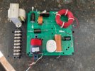
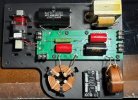
The assembled crossover shown in the first photograph is a physical mockup built with leftover parts, so most of the components are not the final values. Its purpose was to evaluate component spacing, lead reach, magnetic separation, mounting methods, zip-tie locations, and service access before assembling the finished network.
The mockup has already done its job. It revealed several useful changes, including correcting the carrier orientation, improving support beneath the PCB terminal blocks, and revising the connection points for the large axial capacitor so its original leads can reach the board without extensions.
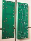
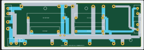
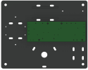
The second image shows the current two-piece design in Fusion 360. The green section represents the circuit board, while the dark 250 × 200 mm carrier provides mounting and restraint for the larger external components.
Positioning the PCB near the center of the major components keeps the high-current connections short and direct. Wide traces and heavy copper carry the crossover paths across the board, while the surrounding inductors, main capacitor, and autoformer connect at nearby edge locations. This minimizes unnecessary lead length, series resistance, and connection complexity without requiring the PCB to support the large, heavy components.
The approach combines the electrical consistency and repeatability of a routed circuit board with the mechanical flexibility of a traditional point-to-point crossover. The PCB carries the smaller components and preserves the electrical topology, while the printed carrier bears the weight of the large components and provides independent mechanical restraint.
Because those larger parts remain external to the PCB, the carrier can be revised without redesigning the circuit board. This makes it possible to accommodate different capacitor packages and various inductor constructions—including laminated iron-core, conventional air-core, and Litz-wire coils—while retaining the same central PCB and electrical connection scheme.
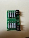
The carrier also provides alternate mounting and zip-tie options. Traditional barrier-style terminal blocks provide familiar screw-down connections, with support beneath the terminal areas so screwdriver pressure is transferred into the carrier rather than flexing the PCB.
The goal is not to create an unrelated crossover or casually alter the established ALK topology. The objective is to package it in a form that is easier to assemble, secure, service, reproduce, and adapt.
This remains a prototype project. I’ll update the thread as the manufactured circuit boards and correct-value components arrive, followed by assembly, continuity checks, electrica measurements, and listening tests.
At this stage, this is strictly a personal development and learning project—not an announcement that I am manufacturing or selling crossovers. I’m pursuing it because the design process is enjoyable, informative, and useful for exploring better ways to package and assemble the network. It may eventually develop into something more, but there are no current production plans. Before manufacturing could even be considered, the design would need to complete physical assembly, electrical verification, listening evaluation, long-term testing, and any necessary review or permissions associated with offering a finished product. For now, the goal is simply to build, test, document, and share what I learn along the way.
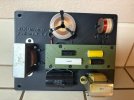
The assembled crossover shown in the first photograph is a physical mockup built with leftover parts, so most of the components are not the final values. Its purpose was to evaluate component spacing, lead reach, magnetic separation, mounting methods, zip-tie locations, and service access before assembling the finished network.
The mockup has already done its job. It revealed several useful changes, including correcting the carrier orientation, improving support beneath the PCB terminal blocks, and revising the connection points for the large axial capacitor so its original leads can reach the board without extensions.
The second image shows the current two-piece design in Fusion 360. The green section represents the circuit board, while the dark 250 × 200 mm carrier provides mounting and restraint for the larger external components.
Positioning the PCB near the center of the major components keeps the high-current connections short and direct. Wide traces and heavy copper carry the crossover paths across the board, while the surrounding inductors, main capacitor, and autoformer connect at nearby edge locations. This minimizes unnecessary lead length, series resistance, and connection complexity without requiring the PCB to support the large, heavy components.
The approach combines the electrical consistency and repeatability of a routed circuit board with the mechanical flexibility of a traditional point-to-point crossover. The PCB carries the smaller components and preserves the electrical topology, while the printed carrier bears the weight of the large components and provides independent mechanical restraint.
Because those larger parts remain external to the PCB, the carrier can be revised without redesigning the circuit board. This makes it possible to accommodate different capacitor packages and various inductor constructions—including laminated iron-core, conventional air-core, and Litz-wire coils—while retaining the same central PCB and electrical connection scheme.
The carrier also provides alternate mounting and zip-tie options. Traditional barrier-style terminal blocks provide familiar screw-down connections, with support beneath the terminal areas so screwdriver pressure is transferred into the carrier rather than flexing the PCB.
The goal is not to create an unrelated crossover or casually alter the established ALK topology. The objective is to package it in a form that is easier to assemble, secure, service, reproduce, and adapt.
This remains a prototype project. I’ll update the thread as the manufactured circuit boards and correct-value components arrive, followed by assembly, continuity checks, electrica measurements, and listening tests.
At this stage, this is strictly a personal development and learning project—not an announcement that I am manufacturing or selling crossovers. I’m pursuing it because the design process is enjoyable, informative, and useful for exploring better ways to package and assemble the network. It may eventually develop into something more, but there are no current production plans. Before manufacturing could even be considered, the design would need to complete physical assembly, electrical verification, listening evaluation, long-term testing, and any necessary review or permissions associated with offering a finished product. For now, the goal is simply to build, test, document, and share what I learn along the way.