• The move to the new server is done. There are some software and database maintenance updates in process. This has us passing the hat around to help out. We appreciate any donations. Seriously, even a dollar helps. The payment page may be found here - https://www.audiokarma.org/support.html

AU-717 regulated PSU voltages

Hyperion

Roobarb & Custard
Subscriber
Every now and again we have someone asking questions about weird regulated PSU voltages for an AU-717 during restoration i.e. with the Driver Modules removed or other boards unplugged. The reason for this is that with the Driver Modules installed they complete a ground path for the whole amplifier including crucially the regulated PSU. If the ground path is interrupted by removing connectors or whole boards the regulated PSU's show weird voltages - because they have lost their ground reference.

If you have a partially dismantled AU-717 and you want to restore the regulated PSU functionality to test that they work after rebuild or for testing other board restoration work, you can do the following.

Assume you have the Driver Modules removed and all the connectors in the below picture are hanging loose. If you connect the black ground connections to the respective ground returns as indicated below this will make the regulated PSU output correct if there are no other faults.

As a test of this procedure I simply stripped the ends of two pieces of insulated wire (of similar thickness to the black and white cables seen below), and folded the stripped ends over to cover the insulation. This makes the stripped cables the right size to (temporarily) fit into the ground wire holes in the female connectors at the top (power amp input connectors), and also into the grey push on connectors with white wire and black wire. (remember these are all hanging loose and disconnected). Ensure the stripped and folded wires can't short on anything!

The regulated PSU voltages should then be correct at ~ +/-33V for each regulator.

NB for safety do not make these connections with the amplifier powered on, and you can do this on DBT, and it should work just as well for this brief test.
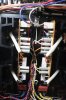
IMG_8671a.jpg

The above is a picture of an AU-717 owned by another AK member ( @sansui au719 ) that I am reconditioning for him. ;)

Any questions, or something not clear just ask. ;)
 
Last edited:
Register to hide this ad
How much tolerance is there for the 33v ? Each of my +/- was off by 1 volt or so, and what would it take to get them closer to spec? Or is this just splitting hairs.
 
How much tolerance is there for the 33v ? Each of my +/- was off by 1 volt or so, and what would it take to get them closer to spec? Or is this just splitting hairs.
Providing all the capacitors that will 'see' this voltage have been replaced with increased voltage ratings, a volt or two either way of 33V isn't going to matter. Ideally of course both of the regulators should output the same voltage, and be balanced i.e. the same +ve voltage as -ve, but it isnt crucially important.

Interestingly, the AU-717 I am restoring has +ve and -ve voltages just over 35V, so I'll be tweaking those to under 35V. How to do this? The zener could be changed for a lower voltage 13V zener, the ones I used are around 13.6V so replacing them with zeners closer to 13V should do the trick. Failing that, and if the +/- voltages are different you can tweak the values of the resistors on the output of the regulators i.e. R27/R29 for +ve and R33/R31 for -ve I think, perhaps others have done this and can confirm the R numbers. ;) NB: If doing so by the resistor method always adjust the +ve regulator first and understand that doing so will also alter the -ve regulator. (the -ve regulator 'tracks' the +ve regulator ;)).
 
Last edited:
Thanks for posting this. Until I read it, I didn't realize the return path was through the signal connector. This eliminates a lot of confusion I've had in the past when working on partially disconnected/disassembled units.
 
Good day.

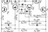
Just to add what John said. PS in AU-717 is so called compensatory type voltage regulator. I will describe the functioning of Voltage regulator just for one channel as the other is the same.
The positive side is consisting of TR01 TR05 which form darlington regulating transistor with high hfe (HFEdarlington = HFEtr01 * HFEtr05). High HFE is needed for higher rejection rate.
TR09 is comparator transistor which drives the regulating darlington transistor (TR05,TR01). Zener D1 is constant voltage against which the comparison is going to be made.
C17 is zener shunting capacitor. Because C17 has relatively large capacitance protective diode D17 is installed in order to protect TR09 from applying reverse voltage to its base emitter junction when power is turned off.
R07 and C09 form smoothening RC filter as this voltage should have as less pulsation as possible to achieve good rejection rate. Sometimes instead of C09 there could be another zener or combimation of zener and capacitor.
Now note at the emitter(actually in our case emitter +R17) of the darlington transistor ( here the same as emitter of TR01) there is a voltage divider R27, R29. to the ground. in ideal and balanced situation when at the junction of R27,R29 the voltage is Vzenner_d1 (in our case around 13V) + Vbe of TR09 (which will be around 0.6V) + some Voltage on R19 (this voltage creates base current of TR09 which keeps it open just enough to make the right output voltage) we will get desired output. Now imagine that for some reason voltage on the output increases, that would lead to increase at the junction of R27,R29 this would lead to opening of TR09 which would result in lowering voltage on collector of TR09 and because collector is connected to the base of darlington transistor (TR05,TR01). This would lead to the slight closure of darlington transistor and as a result output voltage will return to where it was. And opposite is true if voltage at the junction of R27,R29 decreases this would lead to closing of TR09 which would result in increasing voltage on collector of TR09 and because collector is connected to the base of darlington transistor (TR05,TR01) this would lead to the slight opening of darlington transistor and as a result output voltage will return to where it was (increase back). Also between the output of regulator and emitter of TR01 there is a small value resistor R17 which is here for stability.
From the explanation above it should be obvious that in order to manipulate output voltage it is enough to manipulate R27,R29. (I for example) found that combination of 17.4K for R27 and 12.7K for R29 makes the output close to 33V.
Now to the negative side. it works in a very similar fashion as positive, just comparison is with the ground. resistive divider R31,R33,R35 defines negative output Voltage (more precisely junction R33 and R35) .
So in order to achieve good symmetry one can play with value of R31 (stock value 6.8K). For me in the past 5.9 K worked well. increasing the value of R31 will decrease (in absolute value) negative output and opposite decreasing R31 will increase it.
This is it in a nutshell
 
Last edited:
To get the power supply voltages correct for the AU-717 I have here, I changed R27 (and its opposite number in the other regulator) from 18K to 15K - I now have around +/- 34V. I haven't changed any other resistors as I think the voltages are close enough. ;)
 
Last edited:
Basically as i said this is compensatory type of linear Voltage regulator. As i stated above the way this regulator works is "Balancing the bridge" or other words the voltage at the junction of R27, R29 and R19 should be equal to reference Voltage which is in our case is Zener Voltage. This simplification was fairly used by Sansui Engineers. To find out the Voltage at the above mentioned junction point the following formula can be used Vjunction = K * Vout. where K is coefficient and i will describe it bellow and Vout is desired output voltage. Coefficient K is calculated the following way K= Vjunction/Vout = R29/(R29 + R27). How this formula is achieved i will not lay out here but it is simply based on Ohm's law and would be a simple exercise (Hint: current in R29 and R27 can be considered the same)
R29 and R27 are chosen to have high enough value but in such way that it's current would be at least 10 more than base current of TR09 and it easily achieved if hfe of TR09 is high enough.
Let us stick to the values chosen by Sansui engineers. So in our case R29 + R27 = 30K so this would make (substitute values in the above formula for K) K = 12/30 = 0.4. So calculated junction voltage will be Vjunction = 0.4 * 33 = 13.2. In many cases this is what the zener voltage is in reality. However there is a slight issue: the above calculation did not take into account voltage drop on base emitter junction of transistor TR09 which is about 0.5-0.6 volts and in our case Voltage drop at R19 (base resistor of TR09). We can neglect the voltage drop for R19 as the base current will be really really low, but to be more precise we need to take into account voltage drop on base emitter of TR09.

So methodic of calculation:

1. Measure the actual zener voltage Vzener You can do it in existing circuit and it should not change. (Let us assume that we measured it and it was 13.2 V)
2 Add 0.6 to the Vzener. So get Vactual = Vzener + 0.6. (so for our example 13.2 + 0.6 = 13.8V)
3. calcullate K = Vactual/Vout ( for our example K = 13.8/33 = 0.4181818181)
4. using the formula K = R29/(R29 + R27) calcullate new R29 ( in our case we stick to assumption that R29 + R27 = 30, then 0.4181818181 = R29/30K => R29 = 0.4181818181 * 30K = 12.6 (rounded))
5. as we adjusted R29 we need accordingly adjust R27. As we said that R29 + R27 = 30 then R27 = 30 - R29 = 30 - 12.6 = 17.4K

+++++++++++++++++++++++++++++++++++++++++++++++++++++++++++++++++++++

Now to the symmetry. For calculation purposes the junction point of R35,R33 and R21 should have 0 potential for the voltages to be symmetrical. and in ideal case R35 would be equal to R33 + R31. but again there is base emitter voltage drop for TR11 that is why R33 + R31 > R35 this is done to keep TR11 open. Again we can neglect the voltage drop on R21 as the base current of TR11 will be way too small.
however junction point of the R35,R33 and R21 should be at -0.6 Volts instead of 0 Volts. Those resistors are between -33 and + 33 Volts. so total voltage applied between them is 66 Volts. In situation when we expect 0 potential we expect R33 + R31 = R35 => in this case Vr33= Vr31 +Vr33 = ABS(33) (ABS is absolute value) this comes from already familiar formula. R35/(R31 +R33 +R35) and it would be 0.5 However in our case we need to shift it slightly in such way that Voltage on R35 will be ABS(-32.4 )V. So K = 32.4/66 = 0.49090909 . So lets calculate what value R31 should be given that values of R35 and R33 are unchanged. So our equation will be the following : 0.49090909 = 27/(22 + 27 + R31) = 27/(49 + R31) => 0.49090909 * ( 49 + R31) = 27 => 49 + R31 = 55 => R31 = 55 - 49 = 6K (Remember i used 5.9)

However i have another idea which i will test in my next rebuild.
Remember we try to compensate for the forward voltage drop of base emitter junction of TR11. I think what might work fine is installing instead of R31 the forward biased 1N4148(or similar) diode and making R35 = R33 = 27k 1%.


!!!! Remember all resistors have tolerance and in order to achieve desired results one needs to choose tighter tolerances.
 
Last edited:
Had time to check voltages. Right channel is +35.0 -34.1 left +34.3 -33.3 Right zener is 13.33, and that was replaced during rebuild. Is the right side close enough, or should it be adjusted?
 
Is the right side close enough, or should it be adjusted?
Providing the capacitors that will 'see' this voltage have had their voltage ratings increased the above voltages are fine. Obviously as the stock capacitor voltage is/was 35V (for C23, C25 etc on F-2663), it wouldn't be normal to have them running with 35V applied. Manufacturers seem to run electrolytics at up to around 80% of rated voltage, during most recaps these particular capacitors are usually bumped up to 50V rating.
 
Great tip Hyperion, thank you.

On the matter of tolerances for regulated voltages I've taken the view that the component tolerances involved tend to be around 5% and if the voltage is there or thereabouts within 5% or so of the published spec, it's probably fine.

I am aware that this is complicated by things like mains voltage and so would be grateful to know whether there is some "standard" the professional techs use in terms of tolerances here?
 
would be grateful to know whether there is some "standard" the professional techs use in terms of tolerances here?
If there is one I am not aware of it, but with the voltage reference device - namely the zener being normally 5% tolerance, although Leestereo often upgrades zeners to 2%. Most other components (with the exception of electrolytics) are 10%, or 5%, and sometimes 2%, so you can see which way this is going. I think it would be normal to expect between 5% or 10% tolerance on those voltages. If the voltages are close to the spec' voltage of 33V (according to the schematic), the pre-amp output should be within spec', and if the voltages are asymmetric, all it will do is reduce slightly the maximum output voltage of the pre-amp before clipping, which before clipping is easily enough to drive the main amplifier into clipping anyway. As for a normal range of mains voltage variation, it might influence the regulated PSU voltage slightly, but not enough to be significant in my opinion.

That's my feeling on the subject, happy to see alternative views on this.

Just a side note:
During recent reconditioning of an AU-717 I had one of the PSU voltages above 35V. It wasn't like it before, and I did change the zener for a 2% replacement. So I was curious to know why, and removed the zener I had used and tested it with a PSU and a limiting resistor and it behaved the same with voltage a bit high of 13V. I tested several of the other new (2%) ones I had and got the same result. But increasing the value of limiting resistor the closer to the zener voltage of 13V it got, in other words dependant on zener current. I solved my problem by changing one resistor (R27/R28) in each regulator, and brought that 35V down to ~34V - all the other voltages were fine although somewhat asymmetric - no problem. ;)
 
Last edited:
35V is only 6% more than 33V. Completely reasonable, I think.

I’ve been working on an AU-717, and after just cleaning up and fully recapping the F-2663, a la leestereo’s thread, the nominal +/-33V supplies were at +35.8V/-34.9V on one, and +34.8V/-34.2V on the other. But my big rails were running +/-57.7V, across both.
This AU-717 was pretty dirty when I got it, and much of the Sansui glue had gone dark and evil, requiring parts replacement and board hole reaming. :yikes: I am not in the habit of replacing current amplifying transistors outright, but doing so on the driver boards in this unit made them way more stable than before. Maybe my F-2663 needs the same?

edit:I am pulling the F-2663 power supply/protector board today, for transistor/Zener diode/small signal diode replacement today. I will wait until after testing, to see if I need to trim my voltages.
 
Last edited:
Great tip Hyperion, thank you.

On the matter of tolerances for regulated voltages I've taken the view that the component tolerances involved tend to be around 5% and if the voltage is there or thereabouts within 5% or so of the published spec, it's probably fine.

I am aware that this is complicated by things like mains voltage and so would be grateful to know whether there is some "standard" the professional techs use in terms of tolerances here?
Depends on which direction the tolerances of the components go, in relation to each other, as to the actual numbers measured vs. calculated. Some “cherry picking” may be required, depending on how close you’d like to be to spec.
 
After replacing all the semiconductors on F-2663, I measured the nominal +/-33V connections on it, right where the wiring exits the board (same as the first time).
Before-L channel=+35.8V/-34.9V
After L channel+35.6V/-34.6V
Before-R channel=+34.8V/-34.2V
After R channel+34.6V/-34.1V
 
Back
Top Bottom