• The move to the new server is done. There are some software and database maintenance updates in process. This has us passing the hat around to help out. We appreciate any donations. Seriously, even a dollar helps. The payment page may be found here - https://www.audiokarma.org/support.html

AU-D55X service. Where to start

winch

Member
Now that the AU-217II has progressed some I'd like to take a look at this. As posted here the right channel DC offset is out of whack. Also a long-standing problem has been the tone defeat, when in there is a loud "tearing" noise in the left channel.

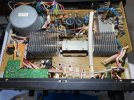
Here's a look inside:
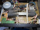
AU-D55X-inside.jpg

It's a little dusty. I don't see any obvious signs of work. It looks like there might be some glue at the base of C1 and C2 (10,000uF 63V).

Partial list of boards:
F3976 Power Amp (rear, center)
F3981 EQ Amp (rear, right)
F3982 Input Selector (upper front, center right)
The upper front, left board with the traces side up is for the meter display. Underneath it is -
F3726 Tone Control (hidden), T mounted on
F3795 Differential Amp (lower front, center) which has the bias trim pots
There are 3 or 4 other smaller boards squirrelled away around the chassis.

Schematic:
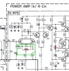
AU-D55X-schem.jpg

I can post more from the manual as required.

So... where to start? Given that my total experience to date is replacing a dozen caps and fuse resistors in an AU-217II.
 
Register to hide this ad
The offset "should be" simple to set if the pot is good. You say you checked the offset so I assume you know how to hook up the meter for the check/adjust.

55x offset.jpg

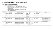
55xadj.jpg

Locate KVR1 on the right channel amp board and gently tweak it a bit and see if the offset changes towards 0, if not go the other way. They are usually very twitchy, small tweak. let it settle, rinse and repeat. It will most likely wobble around a little bit, which is normal.

I would suggest that the tone control issues may be caused by dirty pots & switches in the tone circuit. This amp has the tone controls in the feedback circuit of the power amp.
When you describe the noise is it constant? And when you say the tone control is "IN" what exactly does that mean? The switch is "IN" which I assume defeats the tone controls, or the tone controls are "IN" (switch out).

The small blue box to the right indicates the input to the tone circuit from the output of the power amp, and the top blue box shows the output of the tone circuit to the feedback input of the diff amp. Sansui nicely highlights the audio flow through the system. There are no active devices in the tone circuit which is why I suggested a good cleaning.

Read this: https://audiokarma.org/forums/index.php?threads/the-idiots-guide-to-using-deoxit-revisited.207005/

55xtone.jpg

Be very careful working on live equipment!
 
Last edited:
Hi,
Re the problem you are having with the left channel when “tone defeat” is selected - in this amp “feed forward” design the tone circuits, when selected, are located in the feedback circuits of each channel. If there is an intermittent or “bad” connection in the tone defeat switch then this can cause noticeable issues with the affected channel. This was caused, in my case by an intermittent tone defeat switch. I believe that the switch is a “make before break” design, meaning that there is always a negative feedback circuit connected when engage or disengage the defeat switch. My tone defeat switch was intermittently acting as a ”break before make” action, or it didn’t make a connection in one or other position. I hope the above makes sense! The D33 I was working on would intermittently go “open loop gain” when operating the switch, which certainly livened things up when it first happened (I was using headphones at the time, right ear only)

You will most likely need to give the tone defeat switch a good cleaning, but from my experience on an AU-D33 (same circuit design as the AU-D55X) it is likely that the switch will need to be disassembled for proper cleaning. I was able to use a spare switch I had (from another Sansui) so I cant offer suggestions for disassembly, but there are threads that show the disassembly and cleaning of push switches - but be aware that if you disassemble the switch it has to be reassembled at some point in time, and if that proved challenging (or impossible), you will need to find a replacement switch.

Hope this helps

Cheers
John
 
I would suggest that the tone control issues may be caused by dirty pots & switches in the tone circuit. This amp has the tone controls in the feedback circuit of the power amp.
When you describe the noise is it constant? And when you say the tone control is "IN" what exactly does that mean? The switch is "IN" which I assume defeats the tone controls, or the tone controls are "IN" (switch out).
I realise my description wasn't clear. The noise is intermittent. And actually it is when the switch is "out" that the tone circuit is defeated, which is what I was referring to with "in". I have basically ignored the problem by leaving the tone circuit in the path.

Locate KVR1 on the right channel amp board and gently tweak it a bit and see if the offset changes towards 0, if not go the other way. They are usually very twitchy, small tweak. let it settle, rinse and repeat. It will most likely wobble around a little bit, which is normal.
I gave this a shot, and was able to adjust the left channel to basically 0. Very twitchy! I couldn't reduce the right channel's offset from ~120mV - the trimpot seemed unresponsive, and I blew the power supply fuse before getting anywhere. So I don't know what I'm dealing with on that side. And I'm off to stock up on 3A fuses.

Re the problem you are having with the left channel when “tone defeat” is selected - in this amp “feed forward” design the tone circuits, when selected, are located in the feedback circuits of each channel. If there is an intermittent or “bad” connection in the tone defeat switch then this can cause noticeable issues with the affected channel.
Thanks, my suspicion is the switch too, and I'm not sure if I am game to disassemble it. It's a job that might have to wait until I can secure a spare part myself.
 
I gave this a shot, and was able to adjust the left channel to basically 0. Very twitchy! I couldn't reduce the right channel's offset from ~120mV - the trimpot seemed unresponsive, and I blew the power supply fuse before getting anywhere. So I don't know what I'm dealing with on that side. And I'm off to stock up on 3A fuses.

I hope you were on the correct pot for the right channel. An offset adjustment should not blow a fuse. Now if you were on the bias pot you could have blown the fuse and possibly more. Let's hope not.
 
I hope you were on the correct pot for the right channel. An offset adjustment should not blow a fuse. Now if you were on the bias pot you could have blown the fuse and possibly more. Let's hope not.
I'm pretty sure I was on the bias pot.

So after orienting myself properly with the ID'ing of the trimpots, tonight I replaced the 3A fuse, dialled kVR2 fully counterclockwise like it says in the manual, and powered on again to see if I could get a reading. Immediately I had noise and smoke from the rear right of the power amp board and turned the power off quickly. It was probably 1.5 seconds total. Not good! Any guesses as to what happened? I'll keep inspecting to see if I can locate the damage.
 
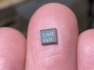
Okay, I've worked out what popped, or at least one thing that popped.

popped_1845.jpg
IMG_7676.jpg

That's Q5L on the protector circuit board, F-3989. Q5R appears intact. At the very least I will need to replace those two.
 
I think at this point it would be smart to read about and build a dim bulb tester, they usually prevent problems like you have experienced.

If you were randomly twirling the bias pot and blew the fuse it is very possible you fried the output transistors. You will need to check them at the very least.

I don't have the AU-D55X schematic here at home, I will have a look at it tomorrow at work and e-mail home as well.
 
It appears my next move is to remove F-3989 and F-3976, depopulate the boards and test and replace components. I might need to do the same with F-3975 but that will be a real cow to get at. Those are the main three boards, on which several circuits are spread out.

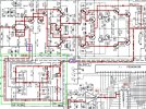
au-d55x_circuits.jpg
The circuits illustrated are:

(j) Control <green>
(k) Power Amp <white>
(l) Protector <pink>
(m) Power Supply <yellow>
(n) Indicator <blue>

Replacing electrolytics and resistors shouldn't pose a problem but the semiconductors are a different story. 2SA992 and 2SC1845 are common enough, but I couldn't find any of kQ9-kQ16 or lQ1-lQ4 in the substitutions thread and if I have to replace them I'm going to need NOS parts or matching advice.

au-d55x_semis.jpg
 
When I restored my AU-D55X the original problem was bad solder joints. Some on the power supply board but mostly connection between boards with the ribbon cables and the daughter boards on the main PCB. I also blew my output transistors trying to test voltages and found out in the end the problem was not with components.
 
It appears my next move is to remove F-3989 and F-3976, depopulate the boards and test and replace components. I might need to do the same with F-3975 but that will be a real cow to get at. Those are the main three boards, on which several circuits are spread out.

View attachment 3305913
The circuits illustrated are:

(j) Control <green>
(k) Power Amp <white>
(l) Protector <pink>
(m) Power Supply <yellow>
(n) Indicator <blue>

Replacing electrolytics and resistors shouldn't pose a problem but the semiconductors are a different story. 2SA992 and 2SC1845 are common enough, but I couldn't find any of kQ9-kQ16 or lQ1-lQ4 in the substitutions thread and if I have to replace them I'm going to need NOS parts or matching advice.

View attachment 3305918
Perhaps a bit ambitious but it would make a good project. I would guess you toasted the output transistors on one channel, you certainly have an issue with the protector board where that transistor lost its face. Never saw one "blown" apart so cleanly. Possibly a cascade failure back into the driver circuit(s).

On the plus side if you remove the 3975 and the 3989 boards you would address the soldering problem areas @GrisPato spoke of. With them out you would have good access to the 3976. Matching is only needed in certain cases and in certain circuits.

If you are digging in deep don't forget the bias and offset pots. Good idea to replace them most of the time on this older gear.
 
In the future I would not follow the fully counterclockwise bias adjustment.
I found that centered on both dc and bias adjustment is your safest approach for adjustment.

In hindsight there was no reason for you to adjust fully counter clockwise on a working unit. You should have just fine tuned it from where it was already set.

I had a similar experience except mine went into protect and would not come out of protect even with adjustment.
The only way it would come out of protect was to center all pots and then adjust from there.
 
Thanks to all for the input.

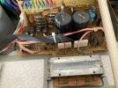
Heat sink has come out, top plate, bar with fins, block which is attached via 4 screws on the underside to the output transistors.

au-d55x_heatsink1.jpgau-d55x_heatsink2.jpgau-d55x_heatsink3.jpg

The power amp board, F-3976 has 5 screws above and one below holding the ground wire to the chassis.

The protector board, F-3989 is not actually sitting loose but has multiple contacts soldered at right angles. Fancy!

au-d55x_f-3986_t-join.jpg
 
Quick update. I extracted the power transistors and tested them, sure enough the right channel pair (kQ15R, kQ16R) are blown. The left channel pair test OK, ~540 ohms B-C and B-E, no short C-E.

Looking at substitutes I found NJW3281G and NJW1302G at Element14 (Farnell). Should I go for these, any other recommendations?

I'll test the other transistors, kQ8-kQ14, lQ1-lQ6 before placing an order.
 
It transpires that lQ5R was fried too, I'm guessing it fried first and lQ5L went out in sympathy because none of the other left channel transistors are bad that I have tested so far. I checked lQ6 as it is a complementing 2SA992, tested OK so it went back in the board.

2x KSC1845FTA have been installed for lQ5L and lQ5R.

After studying the schematic some more and doing a lot of reading, out came kQ8 (2SC1845), kQ9 (2SD438), kQ10 (2SB560), kQ13 (2SD357), kQ14 (2SB527) for testing.

kQ9L and kQ13L test OK
kQ9R and kQ13R test bad
kQ10 and kQ14 both sides test OK.

I also extracted and tested kQ5R and kQ7R (on F-3975), and kQ12R, all tested OK and were reinstalled; and kR32 (39R), kR43 (390R), kR44 (390R) and lR7 (2k2) - these measured OK, but being 1/4W carbon film resistors adjacent to the transistors that blew I decided to replace them on both channels with 1/2W metal film.

I'm very mindful to "fix the problem first" and avoid second-guessing my work.

Given that Q9-Q10 and Q13-Q14 are complementing pairs, do I replace all of them? My planned substitutes are KSC2383YTA - KSA1013YTA and MJE15030 - MJE15031.

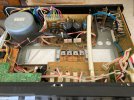
mC1 and mC2 (10,000uF 63V) came out for better access and to remove the glue.
Removed components are marked in orange
Replaced new components are marked in yellow
Reinstalled known good components are marked in green.

F-3976_current-state1.jpg
 
Back
Top Bottom