• The move to the new server is done. There are some software and database maintenance updates in process. This has us passing the hat around to help out. We appreciate any donations. Seriously, even a dollar helps. The payment page may be found here - https://www.audiokarma.org/support.html

Basket Case KA-7002 need some guidance

MBuras

Restoration is an Addiction
I bought it cheap knowing it didn't have sound output. Didn't know until I got it that there were literally parts missing on the amp card and definite signs of being worked on. I've subbed in proper replacements where needed, making sure to check, recheck orientation and pinouts as needed. It mostly matches the board diagram in the SM with some minor differences.

It's been on a DBT since the beginning. I continue to see very high voltages on all the outputs so not willing to risk damage. This could get to be a very long post but I'll try to focus on the outputs for now and we can go over any other issues that need addressed. BTW...I am not a trained EE. Just a guy who's fixed things all my life and receivers/amps have been on my bench for the last 5-6 years. Most make it off the bench and hooked up to speakers. :D

This is an early version KA-7002 with the X07-0027-00 amp card. The relay in this one is normally closed until protection kicks in when you'll hear the relay open. I hear that within milliseconds of powering up the amp on DBT.

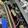
Left outputs are original. Right side are replacement MJ21195/96.

Here are the output readings:

Left channel Q4 NPN
B: +39.1VDC
E: +38.7VDC
C: +42.8VDC

Left channel Q2 PNP
B: +38.6VDC
E: +38.6VDC
C: -43.1VDC

Right channel Q3 NPN
B: +38.7VDC
E: +38.3VDC
C: +42.4VDC

Right channel Q1 PNP
B: +38.3VDC
E: +38.3VDC
C: -43.1VDC

It seems there is something amiss but days of tracing wires and reading diagrams have gotten me no closer to a fix. Hoping there's someone willing to travel down this rabbit hole and guide/teach me.

Thanks,
Mike
 
Register to hide this ad
But your post did make me wonder. So I started beeping out continuity and the cases of both Q4 and Q1 are tied into the chassis. Almost no resistance. And yet I can't find any place where the wires are pinched or the transistor case is touching the heatsink. I'll keep checking tomorrow AM.
 
First things first.. Power supplies,both regulated and unregulated needs to be serviceable. I suspect you have a power supply problem.
 
Are D3 and D4 STV-3H diodes intack on the main amplifier board ?
 
Find Rq 41. It is a 56Ω fusible resistor supplying the -38v supply to both of the amplifiers. Without the -38.3v present it will case the +38.3v to be dominant.And cause the driver transistors to hold the outputs at the positive rail.
 
Are D3 and D4 STV-3H diodes intack on the main amplifier board ?

Yes. They are part of a tag strip attached to the bottom of the heatsinks on each side. Wiring intact and using diode test in circuit they measure 1.4v and 1.5 v (rounded) drop in one direction and nothing in the other with my meter.

IMG_8627.JPG
 
Find Rq 41. It is a 56Ω fusible resistor supplying the -38v supply to both of the amplifiers. Without the -38.3v present it will case the +38.3v to be dominant.And cause the driver transistors to hold the outputs at the positive rail.

It's at the top of the amp card and measures -44VDC on DBT.
EDIT: measures 55-ohm out of circuit

SORRY. The rest of this is going to get wordy.

The top of this card is the section that concerned me from the beginning. Although most of the parts looked period correct it's slightly different than the SM diagram.

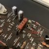
My actual Rq41 (56-ohm) is green as I would expect from a fusible but is installed across parts of the board marked Qq17 (which is supposed to be unpopulated on this version). One end to trace of collectors Qq11 & Qq12. The other end is to the negative of Cq15 (47uf/50v) which wasn't supposed to be populated either but was an original gray Elna. The positive side of Cq15 connects to the top trace which is connected to pin 10 by a jumper wire as shown on the board diagram.

Cq16 which the diagram in the manual shows as 100uf/50v is actually another 47uf/50v and was also original gray Elna. Both since replaced with Nichicon UPW.

One other variation I have since removed is the actual Rq41 marked spot on the board was filled with a 4.7K resistor. It also connected Cq15 negative to the collector trace for Qq11 & Qq12. I pulled it to bring the circuit back to more original condition but can re-install if you think it's needed.

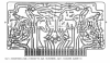
The original board diagram shows Rq41 between the Qq11 & Qq12 collector trace and the Cq16 negative trace. There is now and never was any resistor connecting those two traces. Cq16 negative is alone there until the trace reaches Rq7, Rq8, Rq9, Rq10, Rq21, Rq22.

P.S. At one point I got so frustrated I did try to wire the board exactly as it appears in the SM diagram. It resulted in the DBT being brighter than the sun. Thought that was backwards progress but worth mentioning.

IMG_8629.JPG Screen Shot 2020-08-26 at 8.42.26 AM.png
 
Last edited:
Yes. Just remeasured on DBT.
-43.1vdc but it was still fluctuating a little. The other end was within 0.1vdc.
 
base emitter voltages cannot be the same ....
like this and the other one .
Left channel Q2 PNP
B: +38.6VDC
E: +38.6VDC

or is that a pnp thing i can never get my head around ?
 
What DC voltage are you seeing around Qq5 and Qq6
E
C
B

Qq5
E: +13.1VDC
C: +37.8VDC
B: +13.7VDC

Qq6
E: +13.1VDC
C: +38.0VDC
B: +13.7VDC

BTW these have been replaced with 2N3440 (original 2SC627). The originals were very toasty looking and didn't trust that my simple transistor checker would know they were ok at working voltages.

In case it has anything to do with this I've also observed Rq43/Rq44 are actually two resistors in series to equal 55K. They look new-ish. The schematic and board diagram agree these should be 560-ohm. But when I tried changing them to the proper ohm rating it lit up the DBT. :(
 
emitter resistors might be open circuit . or some other resistors gone open/high

I was down that path given the random output transistors on one channel and "repairs" made to the amp board. I did find one of the emitter resistors on the right channel was bad. Original 0.47 ohm replaced with 0.5 ohm because that's all I have on hand. The other three tested fine in circuit.
 
The only other resistors that are high, at least compared to the schematic, are Rq43/Rq44, noted in the bottom of post #14. They were like that when I received the amp and I just can't verify that the schematic is correct or there was a typo. Trying to change them for the schematic value resulted in DBT lit up bright.
 
Back
Top Bottom