Here are some tips which you might find useful when you have a bias problem.
Below is a schematic snip of a driver board for an AU-517.
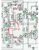
TR06 (centre left) is the bias control transistor, just below it is VR03 the bias trimmer, the transistor and the trimmer are vital to the operation of the bias circuit.
How this bit of circuitry works to control the bias and make it adjustable.
TR05 and TR07 are turned on enough to provide current flow through R23 (from the positive rail) and R25 (from the negative rail). This current also flows through R20, R21 and VR03, these last two present a voltage to the base & emitter of TR06 turning it hard on, corresponding to minimum bias.
With the bias trimmer VR03 wound all the way to the bottom of the track to present all of its track resistance to the circuit TR06 will be turned fully on. With TR06 turned fully on the bases of TR08 and TR11 will be effectively almost shorted together – along the red lines – and so will have insufficient voltage to switch on so, little or no bias current should flow in the output transistors. The voltage present at ‘V’ will be 1 to 2 Volts or thereabouts with the bias trimmer set to minimum bias.
Adjusting Bias
If we then try to adjust bias we will alter the slider position on the track of VR03 in the direction of the purple arrow (upwards). As we do this TR06 will gradually turn off. As TR06 turns off, the voltage at ‘V’ is allowed to increase. As this voltage increases, the voltage across the base and emitter of the driver transistors increases, (green lines) thus gradually turning them on. When this happens the Output transistors also turn on. And with the output transistors turning on, bias current can be measured (as a voltage drop) across the output transistor emitter resistors - This is normal operation. Note that representative voltage drops can be seen across R34 & R35 and also R36 & R37 indicating current flow in the respective pairs of driver transistors.
If you can’t adjust bias:-
i.e. no bias, - OR bias stuck at wrong reading.
– things to check.
First check your power supply voltages (always).
Check that TR05 & TR07 are turning on. voltage B-E=0.6V and their schematic voltages are correct*.
*Use minigrabbers attached with the power OFF then power on to measure the voltage.
Check TR06 – adjust the trimmer and see if the voltage at ‘V’ alters** – if not suspect the trimmer or TR06 faulty. Voltage at ‘V’ will be around 1-4Volts, dependant on bias setting, and amp design.
**Use minigrabbers attached with the power OFF then power on to measure the voltage.
If good up to this point check R29 & R30 (out of circuit - with Ω Meter). Also check R38 & R43 – same procedure. If any of them are high value or ‘open’ they will either starve the drivers of current (R29 & R30), or the Output transistors (R38 & R43). .
If still no-go check the driver transistors, by removing them from circuit and using either multimeter on ‘diode test’ range, or a transistor tester.
Check the Output Transistor emitter resistors, lift one end of each and test.
If still no-go check the Output transistors (remove them) and test as above.
These are the basics, I have tried to explain the operation of the bias circuitry in as simple terms as possible – I hope this helps.
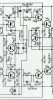
Below is a schematic snip of a driver board for an AU-517.
TR06 (centre left) is the bias control transistor, just below it is VR03 the bias trimmer, the transistor and the trimmer are vital to the operation of the bias circuit.
How this bit of circuitry works to control the bias and make it adjustable.
TR05 and TR07 are turned on enough to provide current flow through R23 (from the positive rail) and R25 (from the negative rail). This current also flows through R20, R21 and VR03, these last two present a voltage to the base & emitter of TR06 turning it hard on, corresponding to minimum bias.
With the bias trimmer VR03 wound all the way to the bottom of the track to present all of its track resistance to the circuit TR06 will be turned fully on. With TR06 turned fully on the bases of TR08 and TR11 will be effectively almost shorted together – along the red lines – and so will have insufficient voltage to switch on so, little or no bias current should flow in the output transistors. The voltage present at ‘V’ will be 1 to 2 Volts or thereabouts with the bias trimmer set to minimum bias.
Adjusting Bias
If we then try to adjust bias we will alter the slider position on the track of VR03 in the direction of the purple arrow (upwards). As we do this TR06 will gradually turn off. As TR06 turns off, the voltage at ‘V’ is allowed to increase. As this voltage increases, the voltage across the base and emitter of the driver transistors increases, (green lines) thus gradually turning them on. When this happens the Output transistors also turn on. And with the output transistors turning on, bias current can be measured (as a voltage drop) across the output transistor emitter resistors - This is normal operation. Note that representative voltage drops can be seen across R34 & R35 and also R36 & R37 indicating current flow in the respective pairs of driver transistors.
If you can’t adjust bias:-
i.e. no bias, - OR bias stuck at wrong reading.
– things to check.
First check your power supply voltages (always).
Check that TR05 & TR07 are turning on. voltage B-E=0.6V and their schematic voltages are correct*.
*Use minigrabbers attached with the power OFF then power on to measure the voltage.
Check TR06 – adjust the trimmer and see if the voltage at ‘V’ alters** – if not suspect the trimmer or TR06 faulty. Voltage at ‘V’ will be around 1-4Volts, dependant on bias setting, and amp design.
**Use minigrabbers attached with the power OFF then power on to measure the voltage.
If good up to this point check R29 & R30 (out of circuit - with Ω Meter). Also check R38 & R43 – same procedure. If any of them are high value or ‘open’ they will either starve the drivers of current (R29 & R30), or the Output transistors (R38 & R43). .
If still no-go check the driver transistors, by removing them from circuit and using either multimeter on ‘diode test’ range, or a transistor tester.
Check the Output Transistor emitter resistors, lift one end of each and test.
If still no-go check the Output transistors (remove them) and test as above.
These are the basics, I have tried to explain the operation of the bias circuitry in as simple terms as possible – I hope this helps.
Attachments
Last edited:


 Thanks!


 .
.