• The move to the new server is done. There are some software and database maintenance updates in process. This has us passing the hat around to help out. We appreciate any donations. Seriously, even a dollar helps. The payment page may be found here - https://www.audiokarma.org/support.html

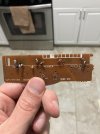
Broken PCB / Trace, but seems salvageable?

BM0127

New Member
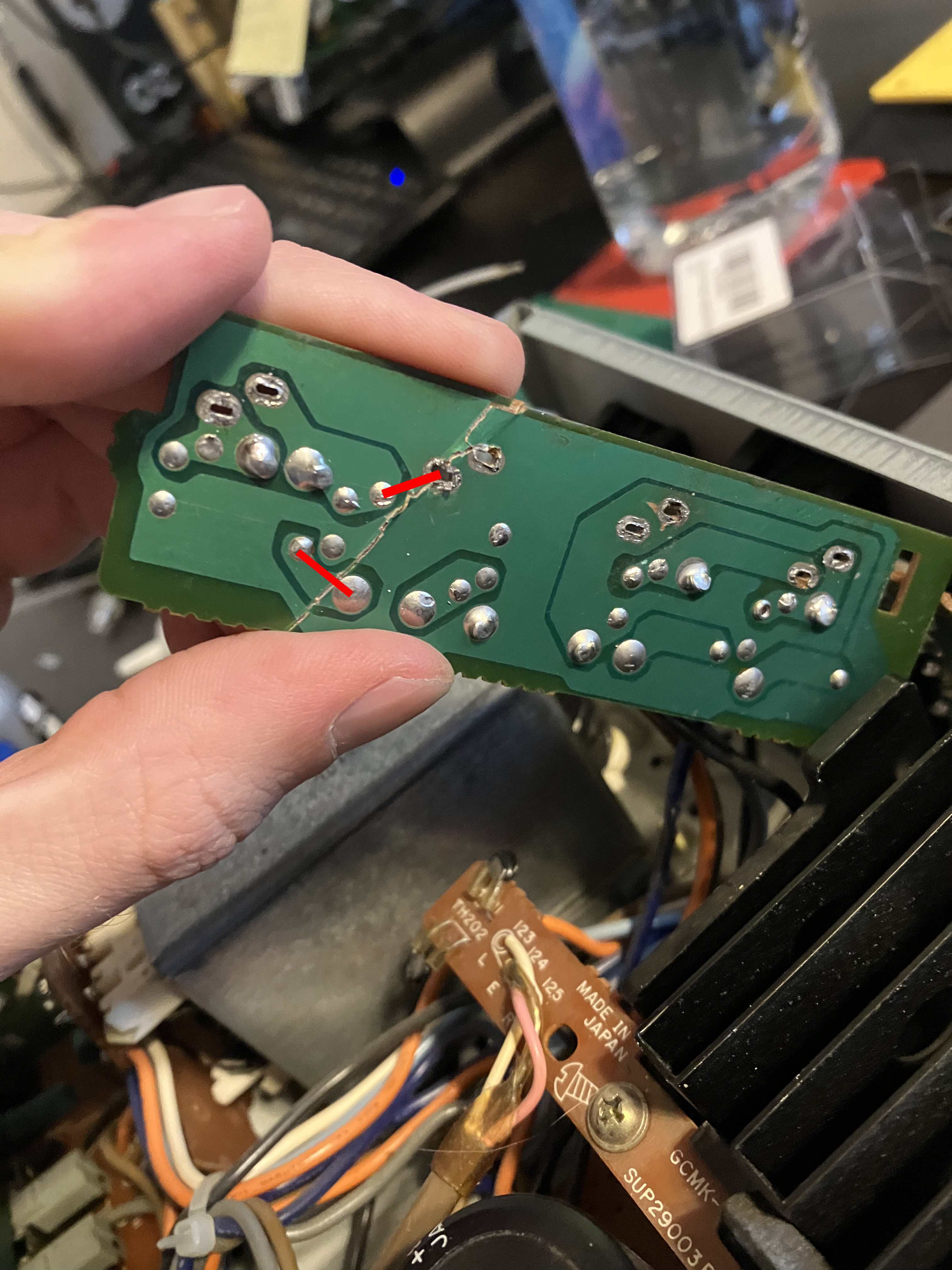
I am replacing the speaker terminal on my old MCS 2250 (essentially a Technics SU-Z400), and broke the PCB when removing the old terminal like a n00b. Real hatchet job.

But seems like I only have one trace I should need to connect? Or are there others? I added a red line where I think I need to address the issue.

Seems most people recommend an epoxy instead of super glue for actually repairing the board itself.

Thanks in advance!

cracked_pcb.jpg
 
Register to hide this ad
Underneath the green that has the largest surface area are copper traces. You will need to make more than one connection. if it is fully broken in two you need to glue it back together epoxy should hold it. Then scrape away the coating that covers the copper either side of the crack. I would use thin copper sheet (foil) soldered over the crack, wire to do this will also work. Check out youtube you will find videos that will help you out.
 
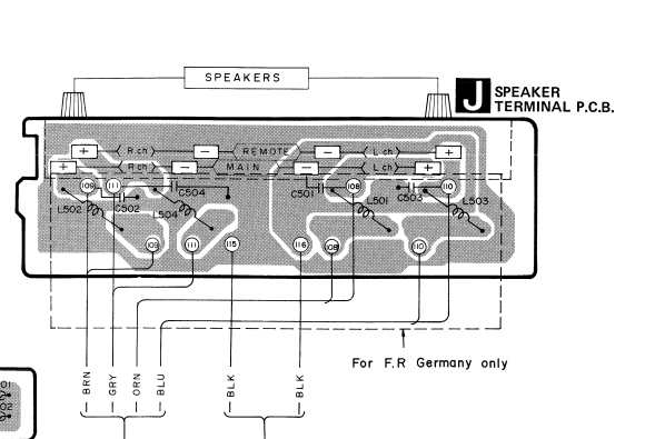
Thanks for the feedback @Alex22. Not sure what you mean "largest surface area"? I've attached the diagram for the board from the manual..

speaker_pcb_manual.jpg


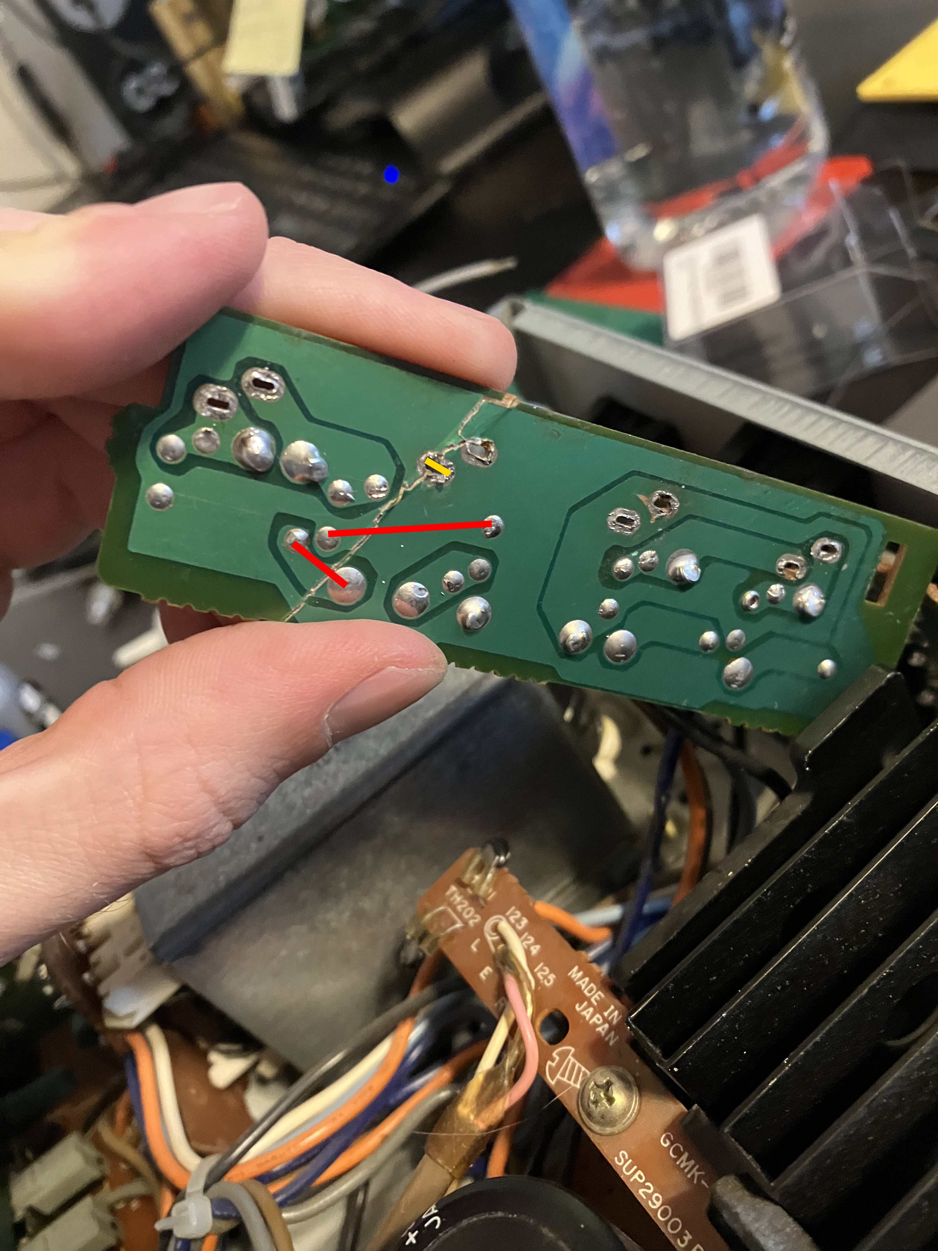
This makes me think I also need to make this second connection? Perhaps I am out of my depth here...

cracked_pcb_v2.jpg
 
In that second photo, the long red line is NOT correct. You want to re-connect the two "islands" of copper that got broken back together. You have the one correct in both photos. Do the equivalent with the large copper island and you're in business.
 
In that second photo, the long red line is NOT correct. You want to re-connect the two "islands" of copper that got broken back together. You have the one correct in both photos. Do the equivalent with the large copper island and you're in business.
@Jefft91 Thanks so much for the detailed feedback -- is this what you're suggesting? Or something to the larger island on the right I have not drawn on yet?
..
cracked_pcb_v3.jpg
 
No, you don't need to connect between any of the components, you need to connect the broken foil. The light green is copper foil covered with solder resist (so the wave solder doesn't stick) and the crack has separated the ground circuit into to pieces. You can either scrape a spot on either side of the crack and solder a wire, or solder a wire between two of the component leads that are soldered into that part of the board.

Don't feel bad, I managed to snap the circuit board in my KA-80 -- something like 20 jumpers to fix it, and I still have an issue with the phono amp PS I have not fixed yet.
 
No, you don't need to connect between any of the components, you need to connect the broken foil. The light green is copper foil covered with solder resist (so the wave solder doesn't stick) and the crack has separated the ground circuit into to pieces. You can either scrape a spot on either side of the crack and solder a wire, or solder a wire between two of the component leads that are soldered into that part of the board.

Don't feel bad, I managed to snap the circuit board in my KA-80 -- something like 20 jumpers to fix it, and I still have an issue with the phono amp PS I have not fixed yet.

Thanks @HPMguy --- so one more diagram lol... Is the second red line I have drawn here what you mean (if I go the wire route)? I also wanted to note the yellow portion there, that will be connected by solder for one of the speaker connections (of which there are 8).

cracked_pcb_v4.jpg
 
That will work. I would epoxy some scrap circuit board to the component side in a couple places to help stabilize it as well after gluing the crack with epoxy as well.

I would also resolder all the connections, I found plenty of cracked ones after I broke that board on the KA-80. The shock wave from the "snap" when the board broke can fracture weak solder.
 
The large foil is the ground plane and although your last picture would fix the board it is is not going to be very strong mechanically. In addition to repairing the single trace that you have in red, I would repair this board by bridging all the way down the crack on the ground plane. Okay don't laugh at my horrible MS Paint editing art work. Follow the scraggly yellow lines in my picture, imagine them as stitches, scrape the green solder mask back 1/4" on either side of the crack where the yellow stitches are located to expose the copper foil and then try to bridge with solder if this doesn't seem to bridge well then lay a few pieces of bare single core wire perpendicularly across the crack, only in those yellow stitched areas and solder those wires on either side. Do not bridge across any open gaps that existed before, only bridge across the actual crack.

Even though the bottom portion of the ground plane will not matter electrically if you correct the top portion I would still repair the bottom most portion of the ground plane, that being the small yellow stitch on the bottom. When combined with a small bit of epoxy on the reverse side of the board as another poster already mentioned if you fully repair the cracked ground plane across the full face of the shown side then this board should be very strong mechanically.


Board2.jpg
 
Last edited:
The large foil is the ground plane and although your last picture would fix the board it is is not going to be very strong mechanically. In addition to repairing the single trace that you have in red, I would repair this board by bridging all the way down the crack on the ground plane. Okay don't laugh at my horrible MS Paint editing art work. Follow the scraggly yellow lines in my picture, imagine them as stitches, scrape the green solder mask back 1/4" on either side of the crack where the yellow stitches are located to expose the copper foil and then try to bridge with solder if this doesn't seem to bridge well then lay a few pieces of bare single core wire perpendicularly across the crack, only in those yellow stitched areas and solder those wires on either side. Do not bridge across any open gaps that existed before, only bridge across the actual crack.

Even though the bottom portion of the ground plane will not matter electrically if you correct the top portion I would still repair the bottom most portion of the ground plane, that being the small yellow stitch on the bottom. When combined with a small bit of epoxy on the top of the board as another poster already mentioned if you fully repair the cracked lower ground plane this board should be very strong mechanically.


View attachment 2840175

This is probably what I would try also. Or epoxy it really well then add a couple jumpers on it to insure a good connection.
 
I agree with both replies, but would also caution you that when you solder the wire for the speaker connection make sure it connects to the trace and isn't an isolated island of copper. It's probably still connected, but certainly worth verifying while you're doing the work.
 
Everyone -- I am back in business! I ended up just going with the wire connection for now but will go for soldering the crack if I run into issues down the road.

Thanks so much for the help to everyone.
 
Use some scrap capacitor lead lengths to bridge the ground plane. Both electrically patent and along with the Epoxy in the joint will keep the joint from flexing excessively.
 
Resurrecting an old thread here...but just want to pass on some findings if anyone else with a MCS 2250 stumbles upon this. On the MCS version of this amp (and apparently non-German models of the Technics versions [see schematic above]) there are no capacitors or any components of any kind. The speaker PCB serves solely as a copper to copper connection. I was having some problems with my shoddy "repair", so I just ended up connecting the 6 wires coming from the main board directly to my speaker terminal wires (I modded mine to use these, which was when I initially damaged the board). The schematic explains it pretty well, you just need to realize the positives have the different locations for the German version...
  • Brown (109): Positive Right Main
  • Gray (111): Positive Right Remote
  • Orange (108): Positive Left Main
  • Blue (110): Positive Left Remote
  • Black (115): Ground Right
  • Black (116): Ground Left
The Positive are all 1:1 connections to the main wires, but the Ground were 2:1.

Previously, my Main channel "worked" but did have some intermittent issues. Remote channel did not work at all. Both are humming now!

I made this fix during a re-cap of the entire unit, and I have to say I am enjoying it quite a bit. A large percentage of that enjoyment may just be pride in the work, but I'll take it.
 

Attachments

  • IMG_2989.JPG
    IMG_2989.JPG
    74.2 KB · Views: 18
  • IMG_2990.JPG
    IMG_2990.JPG
    72.7 KB · Views: 18
Back
Top Bottom