orshad2048
New Member
Hello to all who take an interest in the post here.
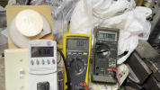
First a bit of background. This is my first go at repairing a vintage electronic anything so a novice level is where I'd place myself at. The equipment that I have to work with to figure out what is going on is a trusty volte meter, a dim bulb tester, and a Techtronic digital oscilloscope (that I have never used and frankly don't know how to use it but that is a future problem)
After quite a bit of looking, watching , reading, and trying to figure out what is going on I've now reached the point where it is time to phone a friend to help me out making sense of what is going on.
I acquired an HK 560 that was working and then stopped working. The person that it was obtained from had never has it serviced and upon opening it up for the first time it did not exhibit any signs that anyone had performed any work whatsoever to it.
Reposted AK HK560 manual link:
http://manuals.harman.com/HK/service Manual/HK560 sm.pdf
The only visible malfunctions upon a first look were the two blown fuses FU2,3 (5A 250V)
After some reading here on the AK site amongst other things it seemed that the most logical place to start was to check the power amp transistors:
I took Q423 and Q421 out of circuit and tested them with the volt meter (in diode test mode). I found that Q423 was dead shorted. Q421 was good as well as Q422 and Q424. All of the good transistors exhibited voltage drops and there were no dead shorts or continuity in a direction that was not normal.
I also removed form circuit and tested both of the bias stabilization transistors Q415, 416
Those were also found to be good by passing my test with the volt meter.
I also tested Q2 (2SC1419(C)) the voltage regulator.
That was also found to be good by passing my test with the volt meter.
So what does one do when one is a novice and do not have items in stock already on hand? You start to look for replacements, find that it is not that simple. You then proceed to spend several weeks in a rabbit hole of what the heck to I replace these broken transistors with. I won't bore the community with that well trodden path of "what do I do here" and get to the point of my first move.
My initial selection for replacing the Q421-424 transistors was based on my internet research NTE382 and NTE383:
I started out the 'repair' by removing Q421- 424, Q2, and both of the bias stabilization transistors Q415, 416 and cleaned the heat sink
I replaced Q421-424 with the NTE transistors being careful to make sure that the case was not grounded to the heat sink by using a non conductive sil-pad (Bergquist SP400-0.007-00-54 THERM PAD 19.05MMX12.7MM GRAY). I also replaced several of the caps on the main power board:
After doing all of that and replacing FU2,3 I then proceeded to power up the unit with the DBT with a 40watt bulb. The bulb went bright and then dimmed and then it illuminated more and stayed that way osculating from more and then less bright. More than the initial dimming but less then how bright it was when it was throttling the inrush current for the filter caps.
I started to do measurements based on the service manual to test the DC offset.
Using hook probes I tested but I did not see the voltage specified at the test points on the volt meter. Looking back at what happed at that time I believe that I did not have the voltmeter set to the 300 ma setting and that was the cause for no measurement. So chalk one up for human error.
I moved the VR403 and 404 pots and did not observe any changes on the volt meter. Being that this is all first time work for me I moved onto the second set of tests for DC voltage on the speaker terminals.
I was not able to observe any DC voltage at the speaker terminals so I figured that all was good and that the absence of DC offset voltage was because of the unit not being fully powered up.
So since the DBT was not showing that there was not a dead short I decided to remove the dim bulb tester and go to full power.
After switching it to full power I with the unit standing vertically I was testing voltages at the underside of the board thinking all was well. After perhaps 30 seconds the first catastrophic failure of Q423 occurred with the top blowing off. The resistor R449 (100ohm 1/2 watt) was taken out as well as FU2,3. Needless to say words were uttered and the smell of electron farts was strong for a while until the place aired out.
So what did I learn from that? In hindsight, well frankly nothing. I tested out various components and not finding anything out of place I replaced the main filter caps with a slightly larger capacitance:
I then replaced the blown Q423, Q421 with another set of NTE382 and NTE383 (I initially purchased a few of them fearing that I make some mistakes) and the blown 100ohm resistor and the blown fuses.
I then removed the following resistors from the circuit and tested them with the volt meter:
Those all tested as good voltage drops with no dead shorts or the ability to pass voltage in reverse and they have been replaced into the board.
I then powered up the board again on a DBT with the same results. Initially bright, then dimmed, then slightly brighter. I made more measurement with the volt meter, I can't recall exactly what they were, and then decided to go for full power. Mistakes were made as Q422 experienced a catastrophic failure. More unhappiness ensued. At least the fuses did not blow and R450 did not burn out.
I then proceeded to replace Q422 and Q424. I also removed the following from the circuit:
Those all tested as good voltage drops with no dead shorts or the ability to pass voltage in reverse and they have been replaced into the board.
I powered the board up one more time after not finding anything that could be causing this behavior with the DBT (same behavior) and then at full power one more time. This time Q423 failed again by popping its top clean off after 30 seconds or so at full power.
What is a fellow to do. I put the project down for a bit otherwise it was going to fly out the window. When I came back it was a back to basics approach. I tested all of the resistors on the power supply board and they all test as good. I've checked all of the diodes on the power supply board (in circuit) and they all show a voltage drop with none of them being blown open.
Since I was out of power transistors I ordered more of them. This time after looking a bit more at the verious scares documentation for the initial specs of the power transistors
I changed my approach based on a cross reference table that I found from the datasheet archive site
 www.datasheetarchive.com
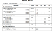
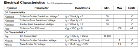
This shows the transition frequency as 15mhz rather than the 8mhz that is the first datasheet you encounter on Google. I decided upon this for the new power transistors as finding a transition frequency in the 15 Mhz range was not possible:
I've replaced Q421 - 424 with the MJE replacements. In addition after doing more research, following the schematic up stream form the power transistors, I started looking closer at the driver transistors:
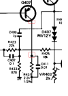
I started by pulling Q417 and Q419 from the board and testing them. I tested the D406, D407 (MV12Y Variator) and they both exhibit the same voltage drop. I did however observe that Q419 had a dead short. I cannot recall if I tested these when I initially blew up the power transistors. Eureka! I though I've zeroed in on the issue, or so I thought.
I replaced Q417 - 420 with:
NTE382
NTE383
(this apparently needs to be a two-part post so the next part will follow)
First a bit of background. This is my first go at repairing a vintage electronic anything so a novice level is where I'd place myself at. The equipment that I have to work with to figure out what is going on is a trusty volte meter, a dim bulb tester, and a Techtronic digital oscilloscope (that I have never used and frankly don't know how to use it but that is a future problem)
After quite a bit of looking, watching , reading, and trying to figure out what is going on I've now reached the point where it is time to phone a friend to help me out making sense of what is going on.
I acquired an HK 560 that was working and then stopped working. The person that it was obtained from had never has it serviced and upon opening it up for the first time it did not exhibit any signs that anyone had performed any work whatsoever to it.
Reposted AK HK560 manual link:
http://manuals.harman.com/HK/service Manual/HK560 sm.pdf
The only visible malfunctions upon a first look were the two blown fuses FU2,3 (5A 250V)
After some reading here on the AK site amongst other things it seemed that the most logical place to start was to check the power amp transistors:
| Q421,422 | 2SD588A |
| Q423, 424 | 2SB618A |
I took Q423 and Q421 out of circuit and tested them with the volt meter (in diode test mode). I found that Q423 was dead shorted. Q421 was good as well as Q422 and Q424. All of the good transistors exhibited voltage drops and there were no dead shorts or continuity in a direction that was not normal.
I also removed form circuit and tested both of the bias stabilization transistors Q415, 416
| Q15, 416 | 2SC1472(K) |
Those were also found to be good by passing my test with the volt meter.
I also tested Q2 (2SC1419(C)) the voltage regulator.
That was also found to be good by passing my test with the volt meter.
So what does one do when one is a novice and do not have items in stock already on hand? You start to look for replacements, find that it is not that simple. You then proceed to spend several weeks in a rabbit hole of what the heck to I replace these broken transistors with. I won't bore the community with that well trodden path of "what do I do here" and get to the point of my first move.
My initial selection for replacing the Q421-424 transistors was based on my internet research NTE382 and NTE383:
I started out the 'repair' by removing Q421- 424, Q2, and both of the bias stabilization transistors Q415, 416 and cleaned the heat sink
I replaced Q421-424 with the NTE transistors being careful to make sure that the case was not grounded to the heat sink by using a non conductive sil-pad (Bergquist SP400-0.007-00-54 THERM PAD 19.05MMX12.7MM GRAY). I also replaced several of the caps on the main power board:
| C4,5,6,7 | 4700mf 50V |
| C8 | 33mf 16V |
| C9 | 47mf 10V |
| C16 | 1000mf 16V |
| C17 | 330mf 16V |
| C14,15 | 470mf 35V |
After doing all of that and replacing FU2,3 I then proceeded to power up the unit with the DBT with a 40watt bulb. The bulb went bright and then dimmed and then it illuminated more and stayed that way osculating from more and then less bright. More than the initial dimming but less then how bright it was when it was throttling the inrush current for the filter caps.
I started to do measurements based on the service manual to test the DC offset.
Using hook probes I tested but I did not see the voltage specified at the test points on the volt meter. Looking back at what happed at that time I believe that I did not have the voltmeter set to the 300 ma setting and that was the cause for no measurement. So chalk one up for human error.
I moved the VR403 and 404 pots and did not observe any changes on the volt meter. Being that this is all first time work for me I moved onto the second set of tests for DC voltage on the speaker terminals.
I was not able to observe any DC voltage at the speaker terminals so I figured that all was good and that the absence of DC offset voltage was because of the unit not being fully powered up.
So since the DBT was not showing that there was not a dead short I decided to remove the dim bulb tester and go to full power.
After switching it to full power I with the unit standing vertically I was testing voltages at the underside of the board thinking all was well. After perhaps 30 seconds the first catastrophic failure of Q423 occurred with the top blowing off. The resistor R449 (100ohm 1/2 watt) was taken out as well as FU2,3. Needless to say words were uttered and the smell of electron farts was strong for a while until the place aired out.
So what did I learn from that? In hindsight, well frankly nothing. I tested out various components and not finding anything out of place I replaced the main filter caps with a slightly larger capacitance:
| C4,5,6,7 | 4700mf 50V | Nichicon | UKT1H682MRD | CAP ALUM 6800UF 20% 50V RADIAL |
I then replaced the blown Q423, Q421 with another set of NTE382 and NTE383 (I initially purchased a few of them fearing that I make some mistakes) and the blown 100ohm resistor and the blown fuses.
I then removed the following resistors from the circuit and tested them with the volt meter:
| Q401,403,405 | 2SC1175(F ) |
| Q411,413 | 2SC1940(L ) |
| Q407,409 | 2SA915(L ) |
Those all tested as good voltage drops with no dead shorts or the ability to pass voltage in reverse and they have been replaced into the board.
I then powered up the board again on a DBT with the same results. Initially bright, then dimmed, then slightly brighter. I made more measurement with the volt meter, I can't recall exactly what they were, and then decided to go for full power. Mistakes were made as Q422 experienced a catastrophic failure. More unhappiness ensued. At least the fuses did not blow and R450 did not burn out.
I then proceeded to replace Q422 and Q424. I also removed the following from the circuit:
| 402,404,406 | 2SC1175(F ) |
| 412,414 | 2SC1940(L ) |
| 408,410 | 2SA915(L ) |
Those all tested as good voltage drops with no dead shorts or the ability to pass voltage in reverse and they have been replaced into the board.
I powered the board up one more time after not finding anything that could be causing this behavior with the DBT (same behavior) and then at full power one more time. This time Q423 failed again by popping its top clean off after 30 seconds or so at full power.
What is a fellow to do. I put the project down for a bit otherwise it was going to fly out the window. When I came back it was a back to basics approach. I tested all of the resistors on the power supply board and they all test as good. I've checked all of the diodes on the power supply board (in circuit) and they all show a voltage drop with none of them being blown open.
Since I was out of power transistors I ordered more of them. This time after looking a bit more at the verious scares documentation for the initial specs of the power transistors
| 2SD588A |
| 2SB618A |
I changed my approach based on a cross reference table that I found from the datasheet archive site
Datasheet Archive: 2SD170A datasheet by N/A
Preview and download the 2SD170A datasheet by N/A on Datasheet Archive.
This shows the transition frequency as 15mhz rather than the 8mhz that is the first datasheet you encounter on Google. I decided upon this for the new power transistors as finding a transition frequency in the 15 Mhz range was not possible:
I've replaced Q421 - 424 with the MJE replacements. In addition after doing more research, following the schematic up stream form the power transistors, I started looking closer at the driver transistors:
| Q417,418 | 2SD667A(C ) |
| Q419,420 | 2SB647A(C ) |
I started by pulling Q417 and Q419 from the board and testing them. I tested the D406, D407 (MV12Y Variator) and they both exhibit the same voltage drop. I did however observe that Q419 had a dead short. I cannot recall if I tested these when I initially blew up the power transistors. Eureka! I though I've zeroed in on the issue, or so I thought.
I replaced Q417 - 420 with:
NTE382
NTE383
(this apparently needs to be a two-part post so the next part will follow)