• The move to the new server is done. There are some software and database maintenance updates in process. This has us passing the hat around to help out. We appreciate any donations. Seriously, even a dollar helps. The payment page may be found here - https://www.audiokarma.org/support.html

Help with Heat Damage on PCB of Mitsubishi DA-A30

angelaudio

Super Member
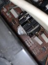
I opened up my Mitsubishi DA-A30 to set the idle current and center potential adjustment and immediately noticed some heat stress marks on one of the PCB boards (CTL-56). IMG_9293.jpeg

It appears that the heat stress is right underneath two 820ohm 2W resistors R313 & R314IMG_9291.png
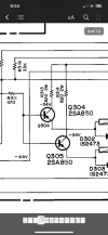
No other part of any other board has any signs of heat stress. What could be causing these resistors to heat up so much as to cause some burning on the board?

In addition to this I also noticed that the right channel cooling pipe has a lot of thermal conductive grease covering it compared to the left channel cooling pipeIMG_9296.jpegIMG_9295.jpeg so I am assuming the right channel is overheating to some degree. What could be causing the thermal conductive grease to be running down onto the pipe from the transistors?

Could the overheating at R313&314 be related to the overheating right channel?

In addition to these questions I need help with the center potential adjustment. The SM gives two pairs of tie points (44&46, 54&56) and says to connect a voltmeter between the output terminals and ground and adjust VR102/VR103 & VR202/203 to obtain a reading of 0+-5mV but does this mean to connect a voltmeter between 44&46 and then 54&56?

Thanks in advance for any help.
 
Register to hide this ad
those are 2 watt resistors knocking -58v down to -34v, i would expect them to run quite warm but wouldn't be overly concerned about it.

if you wanted to buy a couple replacements and install them a 1/4" off the board so air could circulate around them, there would be nothing wrong with that at all

does this mean to connect a voltmeter between 44&46 and then 54&56?
yes. 1st do one channel(44 &46), then do the other channel(54 & 56)

Could the overheating at R313&314 be related to the overheating right channel?

no, they are for the protect relays

What could be causing the thermal conductive grease to be running down onto the pipe
looks like it was just put on like that. it hasn't been dripping on the pcb so i wouldn't consider it "running down the pipe"
 
I wouldn't worry about it. All power handling resistors will get hot and cause some heat related looking spots. As long as it still works and is not giving you any problems, you're fine. If you are worried, just raise 'em up like painttoad mentioned.

Challenge: Open up any 80's to present amps and receivers and you will find heat stress depending how high off of the board power resistors are mounted.

You should see one of my integrated amps. My power supply resistors right off of the diodes have scorched the circuit board black but that's becuase the resistors are close to the board. I have checked it out and the resistors are still spot on spec wise and the solder connections are rock hard.
 
Last edited:
Way too much worrying about those issues. If the board is not charred black it is just normal aging but can be addressed as paintload said.

Look at how much voltage is being dropped across each resistor with a meter and calculate how much wattage that is and size a replacement for that load. The less than 1W from the design is heating the resistor correctly and giving the board a nice tan.

I had a 2W resistor dropping 2.2V and it burned the board to the point of needing to remove the charred area and replacing it with epoxy during the rebuild.

You got nothing to worry about even within 30 years of that kind of issue.

Do the adjustments, put the top on and enjoy it, not worry about it.
 
Last edited:
Thanks y’all for the advice. I had seen another thread about a DA-A30 where a part of the board was charred so I thought maybe mine was headed for the same fate. Thanks for the clarification!

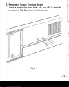
In regards to the idle current adjustment, the SM indicates without saying why, how the output transistor screws are to be removed. Is this necessary for the idle current adjustment or just for removal of output transistors?IMG_9315.jpeg
 
After checking the idling current on the Left channel and seeing that it was well within the given range in the SM (~87mV) and the SM says that it should be between 80-100mV, I decided to leave it that way on that channel. For the Right channel I found it to be ~77mV so I turned VR204 ever so slightly counterclockwise and got it to ~85mV. I know this is not how the SM calls for adjustment, but after realizing the SM diagrams are somehow backwards/inverted and therefore not clear regarding which direction to turn the variable resistors, I decided not to risk doing any damage and just did a fine adjustment.

Is what I did acceptable? Or is it preferable to follow the SM procedure which takes the idle current down to zero, then to 20mV then 50mV, then an additional 10mV somehow resulting in a reading between 80&100mV. Not sure how the idle currents arrives at ~80-100mV after that last adjustment but that’s what the SM says.
 
the service manual gives clear instructions, with clear diagrams and the pcb is silkscreened so that you can orient the unit so that everything matches the diagrams.

they want you to bring the idle current up slowly, let it stabilize, bring it up more. let it stabilize...etc. they have you start at zero because they are assuming that you made a repair and do not want the bias to runaway on startup.

measure and adjust the dc balance while it's open then put the covers on and stay out of it.
 
I had a couple Onkyo M-501 power amps. These when biasing needed to start below the bias needed and had to approach proper bias very slowly otherwise the temp of the heatsink would rise and change the bias, making adjustment difficult.

It took a few tries to get it dialed in properly which means as the instructions state how it is to be done.
 
Back
Top Bottom