• The move to the new server is done. There are some software and database maintenance updates in process. This has us passing the hat around to help out. We appreciate any donations. Seriously, even a dollar helps. The payment page may be found here - https://www.audiokarma.org/support.html

KR-3090 Adjusting DC Offset

mhz

New Member
Hello everyone, I'm working on a KR-3090 and currently looking at bias + DC offset.

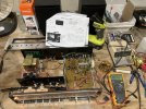
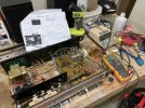
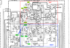
This receiver was on the cheaper end, so adjusting the transistor bias involves swapping a fixed resistor and as far as I can tell there is no adjustment procedure for DC offset. Luckily, transistor bias seems pretty well within spec with 40mV between emitter resistors on the left side and 34mV on the right side:
schematic.png
Left Channel Bias Right Channel Bias
Please excuse the mess...

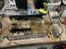
DC bias is not as nice, with 6mV on the left side (good) and -40mV on the right side (questionable):
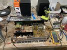
Left Channel DC Offset Right Channel DC Offset

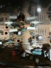
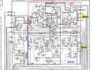
If necessary, it does look like the PCB has spots to add a trimpot in place of the fixed resistor, though I haven't followed the traces to see if it is viable yet considering that the bias offsets are already good. I don't think this would need to be adjusted for DC offset? but can be an option if that is wrong. I assume the PCB was reused for other models that did have (easily) adjustable bias:
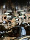
Left Channel Potential Bias Trimpot Right Channel Potential Bias Trimpot

Does anyone have any ideas on what might be causing the DC offset and how to adjust it, or if what I am seeing is really even a problem? Alternatively, does anyone happen to know what models might have shared this PCB (that might have DC bias adjustment)?

Thank you!
 
Register to hide this ad
"Bias offset" is a confusing phrase.

There's DC offset, and there's bias current (which can be calculated from voltage across the emitters with volume at zero and no input...aka idle voltage).

I don't know specs for that unit, but BIAS CURRENT seems high to me. Most amps spec out somewhere between 15-40mA. But the 3090 may well be an outlier.

To address your marginally high DC OFFSET in the right channel, you could try replacing the diff amp transistors with a matched pair (Qm2 and 4). KSA992 would be a good sub.
 
Last edited:
"Bias offset" is a confusing phrase.

There's DC offset, and there's bias current (which can be calculated from voltage across the emitters with volume at zero and no input...aka idle voltage).

I don't know specs for that unit, but BIAS CURRENT seems high to me. Most amps spec out somewhere between 15-40mA. But the 3090 may well be an outlier.

To address your marginally high DC OFFSET in the right channel, you could try replacing the diff amp transistors with a matched pair (Qm2 and 4). KSA992 would be a good sub.
  1. You're right, "bias offset" doesn't make sense
  2. Bias current is from 15mA-110mA according to spec, which would read 14.1mV-103.4mV. It seems like it is in range with 40mV representing about 42mA but good to know that isn't common (service manual gives example for KR-2090 but KR-3090 has same resistor values):
    1769487390927.png
  3. Thank you, I appreciate the suggestion!
 
  1. You're right, "bias offset" doesn't make sense
  2. Bias current is from 15mA-110mA according to spec, which would read 14.1mV-103.4mV. It seems like it is in range with 40mV representing about 42mA but good to know that isn't common (service manual gives example for KR-2090 but KR-3090 has same resistor values):
    View attachment 3685616
  3. Thank you, I appreciate the suggestion!

It's not as high as I thought. I assumed voltage measurement was across just one of the emitter resistors.

But still, I've never seen a range anywhere near that wide for setting the bias current. Live and learn!
 
Just an update - got some time to replace Qm2 and Qm4 with a pair of KSA992 I had on hand. Their gains seemed to match well enough with hfe readings like 345 vs 351 if Harbor Freight multi-meters are to be trusted. DC offset has gotten worse with about 70mV on right side. Maybe I will try another pair, or though it seems unlikely maybe something else in the circuit like a resistor is not well matched. Ran out of time to keep messing with it.

Something I did notice is that with volume turned all the way down (as it should be for these measurements) I am getting 143mV on the base of Qm3 which should ideally be zero. For the left channel Qm1 only has 66mV on the base. I wonder if the signal before the first amp stage could be causing the offset.

Will experiment more when I have time.

For future reference to anyone reading this example helped me understand this part of the circuit a little bit better: Two Stage Differential Amplifier with Negative Feedback
The example is almost identical to this schematic if you invert the polarity of all the transistors and swap the positions of the transistors in the second stage.
 
I got lost after the initial section! But I know that with dual differential amps the common solution of replacing transistor pairs seems much more hit or miss.

Might be worth tracking down the voltage aberration.
 
I ended up giving up on this after awhile and put the receiver aside for a few months, but started to take a look at it again this weekend. Some updates:

I realized that matching hfe readings /w a harbor freight multimeter is NOT a good way to match transistors, and ended up building a "Fritz matching circuit" to get them as close as possible. After ordering 100+ KSA992 transistors on a tape and matching a pair to within 0.01-0.02mV difference on the circuit, I was able to replace Qm2/Qm4 once again to bring the right channel DC offset back down to 40-50mV after making it worse with my original replacement. The original transistors measured very close on the matching circuit as well and I no longer think the differential pair matching was really the issue.

The only thing that really stands out to me between left channel (good) and right channel (bad) is weird voltages at the base/emitter of Qm2 in right channel compared to that of Qm1 on left channel:

kr3090-readings-1.png
Though I do not understand where it would be coming from since signal path before the Cm4 coupling cap is basically 0V and the other end of Rm8 and Cm6 is also 0V.

I did some rough in-circuit testing for resistances of Rm9, Rm14, Rm10, Rm12 and although in-circuit testing is not reliable the readings all matched pretty well.

Other things I have tried:
  • I previously replaced Cm3/Cm4 (which couple the pre-amp stage to amp input stage) with WIMA film caps. I tried swapping Cm4 back to the original tantalum capacitor, made no difference.
  • Just for the sake of trying I replaced Qm6/Qm8 with a matched pair of KSC1845, made no difference for better or worse.
Any ideas on other areas to check?
 
Even if the differential pair transistor are exactly the same, you will have inherent DC offset because the of the choice of components they used. Assuming that each bjt diff pair has the same Hfe, Ic thus Ib will be the same. The resistors in the bases, where the current flows, are not. The input base current (Ic/hfe) for Qm1,(2) flows through Rm7,(8), (100k). The base current for Qm3,(4)flows through the series combination of Rm21(1k1) + Rm25(56k), and Rm22+Rm26.
Base current, even though the same, flows through these different values of base resistors, will create a small voltage difference because they are not the same. If you were to change Rm7(8) to be more like the feedback source resistance 56k+1k1 you would have better DC balance.
 
Last edited:
Observe R33 (left channel) and verify the value. Consider replacing that with a 330Ω metal film and parallel that with a 500Ω trimpot. That could allow adjustment of output bias and still retain some measure of failsafe protection should the trimmer pot have a failure.

If you notice the asterisk * next to that resistor, that is an indicator of bias adjustment component(s), but instead of experimenting with fixed resistor values a trimmer makes adjustment almost infinite.

In looking at the documentation, it does not appear that R33 is a printed resistor. Even if it were one of those, the carbon trace could be cut and mounting holes drilled to accommodate a through-hole mounting for the replacement parts. In this case, holes are present, and additional holes in one of the traces are adjacent to the thermal compensation diode stack.
 
Back
Top Bottom