• The move to the new server is done. There are some software and database maintenance updates in process. This has us passing the hat around to help out. We appreciate any donations. Seriously, even a dollar helps. The payment page may be found here - https://www.audiokarma.org/support.html

Marantz 2245 left channel puzzle

AngelAT

Well-Known Member
Hello AKs,

I would like to ask you for advise because I just cannot figure it out
I am finalizing my work on a 2245 and I came to a place where I ran out of ideas.
The problem is as follows:
Left channel shows signs of short when J761 is connected to the minus of C008. When connected and unit turned off the testing device shows h003 and h004 as shorted and when unit power on, DBT shines bright. When j761 is not connected end transistors measure ok.
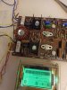
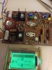
IMG_20220723_210106.jpgIMG_20220723_210033.jpg
I have replaced c006 and c007 with nichicon fine gold 10 000 uf/63v and I believe I have connected the j761 (white) correctly to the minus.
IMG_20220723_210113.jpg
Otherwise, I have reworked both channels and I just wonder if this left channel is missing a capacitor (500 pF) at the bottom and also a jumper cable which I believe are present at right channel. Also I cannot see these at the schematic.
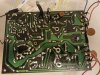
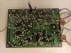
IMG_20220723_210157.jpg

I checked all single transistors and they are ok. Diodes are also ok. New emitter resistors.

Any ideas are welcome! Thanks in advance!
 
Register to hide this ad
Are there mica insulators between the output transistors and the heatsink? Even if there, one may be damaged and allowing the case of the output transistor to short to the heatsink.

The wiring to the main filter caps looks correct.
 
Thanks guys for stepping in!

Micas are new. Further more, this same thing happens when I check without the heatsink...

When I use only the right channel, the DBT is behaving ok. Is this what you mean, ocdecio?

Problem occurs when I connect the minus of the big filter cap. This messes up the two end transistors. And this happens with old original ones and also with mj21193/4. They measure ok out of circuit and also in circuit but when not connected to minus of the filter cap.

Any ideas?
 
Thanks guys!
This I checked several times. If the schematic I use is correct, at J761 I have sj2513/mj21194 (NPN). Respectively, at J753 - sj2514 and mj21193 (PNP).
Am I/schematic right?
Same thing I did on the right channel.
 
I understand! And since smo was already there this might have been changed. But at the end, pins should count, right? I mean same pins for PNP and NPN and at the back one can play with the wires of the output transistors and change top and bottom location.
Never the less I will exchange places and see what happens...
 
Never the less I will exchange places and see what happens...
I don't think that you want to do that! :eek: Why don't you just trace the wires to the two transistors and check it against the schematic.
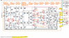
What is your S/N? Apparently the wiring is different depending on S/N.
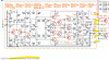
upload_2022-7-25_7-42-43.png

upload_2022-7-25_7-51-23.png

upload_2022-7-25_7-45-0.png
 
Last edited:
Hard to tell from the pic, but looks like you added a jumper to a trace?
Also some solder joints look like they could be suspect.
Reflow the joints and check continuity of your jumper.
 
Definitely don't just swap the outputs to see what happens. Like @dankik said, compare the outputs to the schematic that is appropriate for your serial number. I only mentioned the output position on the heat sink because it is a somewhat common mistake that usually ends up with a kapow if not on a DBT.
 
Thanks for the ideas, guys!

I believe mine is the third schematic, as it's number is above 50 000. I am also following the schematic and this is the way I connect the output transistors. Further more, right channel is done the same way and it operates correctly, biased ok.
But someone has been in this left channel and I just don't know...
I checked the jumper and it's ok, but should there be another jumper starting at H758 and H759 and a 500 pF capacitor. These are not on the schematic but are present at the right channel.

I will not change the places as I believe I put them according to the schematic.

But I will check for bad soldering joints.

Generally, I wonder what might flip when I connect the filter caps?...
16587770917358266374692901996799.jpg
 
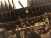
One thing I noticed in your last photo -- the bias transistor is the old can type that was used on the earlier models. I don't know for sure when they quit using it and went to a flat style transistor, but I believe it was at least under serial number 20,000. Does your right channel have the round bias transistor or the flat one? If it is flat, then this board may be a very early one that was swapped in. The bias transistor is the one that attaches directly to the heat sink.
 
Is the bias set way too high?....maybe turn the trimmer down and see if that helps. I might've had that happen to me once and it looked like a short ;)
 
One thing I noticed in your last photo -- the bias transistor is the old can type that was used on the earlier models. I don't know for sure when they quit using it and went to a flat style transistor, but I believe it was at least under serial number 20,000. Does your right channel have the round bias transistor or the flat one? If it is flat, then this board may be a very early one that was swapped in. The bias transistor is the one that attaches directly to the heat sink.
Wow, Steven!
You are a genius! Never thought about that...
But still, this does not help. Comes out both channels are with the can style. Though the serial number is above 50 000. Could not find any production date stamp.
Right channel fixed and working according to the schematic for the latest version...
IMG_20220727_072327.jpgIMG_20220727_072237.jpg
Tonight after work I will take out the right channel and check it thoroughly.
 
Though the serial number is above 50 000. Could not find any production date stamp.
Old post describing where to find the production date on a 2245.
upload_2022-7-26_23-42-33.png
upload_2022-7-26_23-57-35.png
"19740515" is manufacturing date of May 15 1974.
 
Last edited:
Thanks dankik!
Mine is missing the stamp where they usually put them. But I will examine again once back home.
As mentioned before, it might come up that the power amps might have been added later.
 
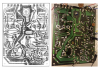
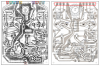
I looked at the Power Amplifier P750 board layout in you photo and it seems to match with the one in the SM.
Check out R788. It goes from J754 to R788 on your board photo and the SM board layout. This circuit configuration matches with only the First schematic (S/N 1001 - 3300).
You should check the Right channel to see if the board matches the same layout below. Maybe you have a mixed vintage set of boards and so this one is wired wrong (causing a short)?
Take a photo of the front and back side of the Right P750 board and the power transistors where the colored leads attach and post.

upload_2022-7-27_8-50-11.png

Board layout vs Schematic. (colors have no relationship to the wire colors) Trace the wires from you P75 (L) to the power transistors vs. schematic and board layout to make sure they are connected to the right places.
upload_2022-7-27_9-58-15.png

If your S/N is correct, then maybe someone tried to substitute an old board in for a "new" board and got the wiring wrong?

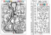
Here is a comparison with a later version of the board. Note the different connector arrangement and components that are connected to the pins. Also, the PCB P/N is different: 2819007-0 vs 2818007-0.
upload_2022-7-27_10-40-9.png
 
Last edited:
Back
Top Bottom