
• The move to the new server is done. There are some software and database maintenance updates in process. This has us passing the hat around to help out. We appreciate any donations. Seriously, even a dollar helps. The payment page may be found here - https://www.audiokarma.org/support.html

Matching TO 3 output transistors. MJ15022

Hifibythekg

Super Member
Hi, looking for some advice please.

I'm replacing output transistors in a Rotel RA913 and need to match them.
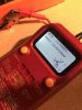
My cheap transistor tester displays the following for the four transistors:

B =62
Uf = 554mV

B =72
Uf = 548mV

B =62
Uf = 555mV

B =58
Uf = 556mV

Which number(s) should I be best trying to match, B or uF?

I presume the two closest are put in one channel and the next closest matching in the other channel?
 

Attachments

  • IMG_6964 copy.jpg
    IMG_6964 copy.jpg
    87.6 KB · Views: 41
Register to hide this ad
Thanks Inductor for the advice and reassurance.
For matching transistors is it the B or the uF measurement that’s matched?
 
It depends on the application. In a power amp, if you have multiple output transistors that are paralleled for increased current output then the Vf matching will decrease current hogging by one output. This is usually mitigated by using emitter resistors to balance the output currents. I looked at the schematic, this amp has single output transistors in the output stack. No benefit to matching Vf (Vbe).
If you want to match B (Beta, ß or hFE) you are going to need more than four transistors to chose from, but you already have 2 that match and 2 more that are way out of match. At about $7 each you are probably not wanting to buy 20 or more to get closer matches, that will not provide a real benefit anyway. Since this amp uses negative feedback you won't get much benefit from matching output transistor B either.
If you are really wanting to match them you will need a curve tracer that can handle power transistors, and a bunch of them to sort through. hFE varies with collector current, the tiny current that tester uses is not anywhere close to the operating current the outputs will carry under load.

This is, basically, a long-winded way of saying the same thing inductor did.

YMMV
 
Thanks Merlynski. Appreciate your effort in giving lots of background in the explanation and for looking up the schematic to tailor it to my situation, very helpful. Now can’t help pondering whether should I put the best matched pair together in one channel, or have both channels as ‘unmatched’ as possible..?
 
I think that what the responses actually pointed out is that your readings with the low cost, low current, transistor tester are pointless and don't tell you how these transistors match.
Consider that the tester only drives the transistors to a current of a few, single digit, mA. Very likely, well below their nominal biasing current draw.

Although a curve tracer has significant benefits (and a crazy sexy name) it might be more relevant to use a DMM (good quality) to measure Ic for the output transistors with a base current of about 10-20mA and an actual R load that causes Ic to be in the 300-500mA range. That would be safe to do, perhaps even without a heatsink, and would cause the transistors to get warm, so you can measure Ic in more realistic conditions (higher current, higher temperature) that relate to their operation in an output stage.

Regarding matching beta, (β / hfe) I have the hunch that it's important to do so between the NPN and PNP counterparts - to be able to get a symetric output from the output stage.
Regarding Uf, with most class AB output sections being biased to slightly higher than a nominal Vbe, I assume they are almost irrelevant.

I may be incorrect in the above - would be happy if someone more knowledgeable can correct me or confirm my notions.
 
I think that what the responses actually pointed out is that your readings with the low cost, low current, transistor tester are pointless and don't tell you how these transistors match.
Especially for power transistors. I believe those testers do have utility with small signal transistors. I have and use one.

Regarding matching beta, (β / hfe) I have the hunch that it's important to do so between the NPN and PNP counterparts - to be able to get a symetric output from the output stage.

I once thought so too.
The Rotel RA913 has a Class AB quasi-complementary symmetry output architecture. Aside from the very small Class A area of operation near 0v output the output transistors conduct only during their own half-cycle, and are in cutoff during the other half cycle, The positive side sends current through the load during positive voltage signal conditions, the negative side sends current through the load on the negative voltage signal conditions. Since they are not both conducting output current at the same time, matching hFE has no effect on the output. The negative feedback from the differential amp takes care of the difference in gain between the positive and the negative excursions. The driver transistors are npn and pnp, which are pretty much impossible to match.
The output distortion spec for the RA913 is only 0.3%, pretty dismal by today's standards.

Here are a couple of methods for testing/matching transistors:

DIY Transistor Matching Circuit | Audiokarma Home Audio Stereo Discussion Forums

This is a link to Elliot Sound Products: https://sound-au.com/index.html
He requests links go only to his main page and I have honored that request. You will have to click on the Projects, and select Project 106.
There is LOTS of great real world information on his site, look it over.

EDIT: also look at Project 31.
 
Last edited:
Thanks Merlynski, great links.
Body of knowledge continues to build.
So, in my particular situation it would appear that in whichever order I should place my four new MJ15022's there will most likely be no audible difference, and any quantifiable difference in performance would be of no significance.
Hope I've got that right...
 
You got that right!
Also go to Project 31 on the ESP site, that transistor tester can handle power transistors. I have the parts on hand to build one of those.
 
Take the four transistors to somebody who has nothing to do with this project and have them pick two (don't watch), then put those in one channel, and the other two in the other channel.
:jump:
 
I think that what the responses actually pointed out is that your readings with the low cost, low current, transistor tester are pointless and don't tell you how these transistors match.
Consider that the tester only drives the transistors to a current of a few, single digit, mA. Very likely, well below their nominal biasing current draw.

Although a curve tracer has significant benefits (and a crazy sexy name) it might be more relevant to use a DMM (good quality) to measure Ic for the output transistors with a base current of about 10-20mA and an actual R load that causes Ic to be in the 300-500mA range. That would be safe to do, perhaps even without a heatsink, and would cause the transistors to get warm, so you can measure Ic in more realistic conditions (higher current, higher temperature) that relate to their operation in an output stage.

Regarding matching beta, (β / hfe) I have the hunch that it's important to do so between the NPN and PNP counterparts - to be able to get a symetric output from the output stage.
Regarding Uf, with most class AB output sections being biased to slightly higher than a nominal Vbe, I assume they are almost irrelevant.

I may be incorrect in the above - would be happy if someone more knowledgeable can correct me or confirm my notions.

I have done the higher power beta measurement using a homemade setup with meters and Ic at maybe 4 amps or so. You can do this long enough to get readings without needing a heat sink.

As for attempting to match PNP and NPN, there will be large differences. The fix is a properly designed circuit that can compensate for the variation.
 
Can you please elaborate on the subject of matching PNP and NPN? Why would there be large differences when trying to match complementary pairs of PNP/NPN transistors?
I would think that a tesdbed "output" section circuit with a bias spreader included would provide a working condition for the transistors to show their characteristics. Perhaps alternating the PNP and NPN in operation?
 
Can you please elaborate on the subject of matching PNP and NPN? Why would there be large differences when trying to match complementary pairs of PNP/NPN transistors?
I would think that a testbed "output" section circuit with a bias spreader included would provide a working condition for the transistors to show their characteristics. Perhaps alternating the PNP and NPN in operation?
That is a physics question that there is not space (or time) for in this venue, but it has to do with the nature of the doping chemistry and the covalent bonding in the formation of the PN junction. The NPN and the PNP are not 'mirror' images, they have different majority carriers, electrons in an NPN; holes in a PNP. It took years for the scientists to figure it out and the engineers to make it work to get them close enough to be functionally complementary, especially in high power transistors. Wikipedia has a basic article: https://en.wikipedia.org/wiki/Bipolar_junction_transistor.
 
I understand these differences but complementary pairs of NPN / PNP transistors should have symmetrical properties (same gain, same Uf, same SOA, etc). Just driven with opposite polarity. Their output should be a mirror image of each other. That's what I was talking about for matching these.
 
I understand these differences but complementary pairs of NPN / PNP transistors should have symmetrical properties (same gain, same Uf, same SOA, etc). Just driven with opposite polarity. Their output should be a mirror image of each other. That's what I was talking about for matching these.
Well, sometimes 'should have' and 'actually have' don't match. We would all like them to match perfectly, but in reality they don't.
 
Look up some spec sheets for MJ15001-02, 03-04, 15015-16, 21993-94. In each case, the beta listed in the table is identical for the PNP and NPN, but then look at the graphs. Most of those spec sheets will have the graphs side by side and the PNP and NPN will be quite different. Additionally, frequency is a factor and the gain bandwidth product will be different.
 
Looked at a few of my TO-3 transistors that are marked for measured beta.
MJ21195 and 21196 - NPN transistors are 60-63 and PNP are 71-78.
MJ2955 and 2N3055 - NPN are 73-90 and PNP are 52-63.
MJ15022 and 23 - NPN are 59-63 and PNP are 69-75.
 
I agree with inductor; there's no real need to match output transistors since in complementary output stages, the transistors are operated as emitter followers, where voltage gain is a tad less than 1 due to the 100% feedback you get using a transistor that way. That tends to null out differences.
 
Back
Top Bottom