Hello,
I have a 326BEE with a problem that's proving pretty difficult to pin down. The first thing I noticed a little pop from the unit and the left channel went out. The only damaged component I could find was R250, which looked like it had blown, but was maybe just scortched and was still testing as 10ohms. I replace it anyway and stood it off the PCB a bit for better cooling. There were also a number of electrolytics that looked cooked and I replaced all those (many tested bad). The film capacitor in series with R250 (C172) I also checked and it's ESR of 24ohms seemed high, so I replaced it with a wima MKP10 I had. Everything I replaced on the left channel I also replaced on the right to maintain symmetry.
After doing all this the left channel was still low. Feeding in a 50mV RMS 1kHz sine to both left and right main inputs, I was getting 1.3V on the right channel and 200mV on the left into 8ohm loads. In attempting to narrow down which part of the amp contained the fault, I swapped the vertical mounted boards between channels, and this is where things get confusing. I'll refer to the seperate PCBs as Board L and Board R, indicating their original positions in Channel L and Channel R.
With Board L in Channel L, as I mentioned previously the outputs are Channel L: 200mV, Channel R: 1.3V. The amp is drawing almost 120W in this configuration, and I'm unable to get the channel L bias voltage below 80mV. Channel R bias is fine. With the input signal removed the amp draws about 100W.
With Board L in Channel R, I get 1.3V on channel R, and 200mV on channel L. The amp draws about 42W with the signal, and 35W without. Bias voltages on both channels can be brought into spec. Note that the 35W idle power is where the amp is supposed to be, according to the manual.
So the low output problem follows Board L, but there is also something funny about Channel L which Board L prevents the bias from being set and causes a bunch of current to get dumped through Q151 and Q145.
I've gone over Board L multiple times at this point. I've pulled every transistor and tested them, checked every diode and resistor. I think I'm going to start swapping parts between Board L and Board R to see if I can narrow it to a component, but even if I find that, it's only half the problem, because what is going on with the rest of channel L that causes all that excess current dump. I have temporarily fitted sockets for Boards L and R so I can easily remove and swap them. I'm thinking I might want to also make a little extender cable so I can measure currents out on each pin.
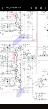
Does anyone have any ideas here? Amplifier schematic attached
I have a 326BEE with a problem that's proving pretty difficult to pin down. The first thing I noticed a little pop from the unit and the left channel went out. The only damaged component I could find was R250, which looked like it had blown, but was maybe just scortched and was still testing as 10ohms. I replace it anyway and stood it off the PCB a bit for better cooling. There were also a number of electrolytics that looked cooked and I replaced all those (many tested bad). The film capacitor in series with R250 (C172) I also checked and it's ESR of 24ohms seemed high, so I replaced it with a wima MKP10 I had. Everything I replaced on the left channel I also replaced on the right to maintain symmetry.
After doing all this the left channel was still low. Feeding in a 50mV RMS 1kHz sine to both left and right main inputs, I was getting 1.3V on the right channel and 200mV on the left into 8ohm loads. In attempting to narrow down which part of the amp contained the fault, I swapped the vertical mounted boards between channels, and this is where things get confusing. I'll refer to the seperate PCBs as Board L and Board R, indicating their original positions in Channel L and Channel R.
With Board L in Channel L, as I mentioned previously the outputs are Channel L: 200mV, Channel R: 1.3V. The amp is drawing almost 120W in this configuration, and I'm unable to get the channel L bias voltage below 80mV. Channel R bias is fine. With the input signal removed the amp draws about 100W.
With Board L in Channel R, I get 1.3V on channel R, and 200mV on channel L. The amp draws about 42W with the signal, and 35W without. Bias voltages on both channels can be brought into spec. Note that the 35W idle power is where the amp is supposed to be, according to the manual.
So the low output problem follows Board L, but there is also something funny about Channel L which Board L prevents the bias from being set and causes a bunch of current to get dumped through Q151 and Q145.
I've gone over Board L multiple times at this point. I've pulled every transistor and tested them, checked every diode and resistor. I think I'm going to start swapping parts between Board L and Board R to see if I can narrow it to a component, but even if I find that, it's only half the problem, because what is going on with the rest of channel L that causes all that excess current dump. I have temporarily fitted sockets for Boards L and R so I can easily remove and swap them. I'm thinking I might want to also make a little extender cable so I can measure currents out on each pin.
Does anyone have any ideas here? Amplifier schematic attached