

After having had a bad experience with my R-1, blew the left channel, I just had to dig deeper into the problem.
I found a difference between the schematic and the actual main board.
The component in question is VR301 R and L. (Bias control)
Here is the question: which of the two situation is correct?
My guess: VR301L is wrong (as tinkering with it blows the whole left side MOSFETs).
I don't have enough knowledge to come to the right answer.
Who can help?
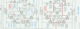
First photo is part of the schematic to situate the VR301
Second photo is part of the schematic what is actually on the PCB.
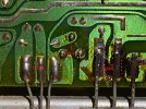
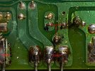
Photo 3 and 4 the back of PCB as it is now (the flux has been removed...)
I found a difference between the schematic and the actual main board.
The component in question is VR301 R and L. (Bias control)
Here is the question: which of the two situation is correct?
My guess: VR301L is wrong (as tinkering with it blows the whole left side MOSFETs).
I don't have enough knowledge to come to the right answer.
Who can help?
First photo is part of the schematic to situate the VR301
Second photo is part of the schematic what is actually on the PCB.
Photo 3 and 4 the back of PCB as it is now (the flux has been removed...)
Attachments

Last edited:
