• The move to the new server is done. There are some software and database maintenance updates in process. This has us passing the hat around to help out. We appreciate any donations. Seriously, even a dollar helps. The payment page may be found here - https://www.audiokarma.org/support.html

Pioneer SA-7500 II - DC Offset

Moncho

Member
Hi guys,

As the title says, the amp has DC Offset and I don't know the cause, so I'm publishing this post, hoping that someone can help me, because I've run out of ideas (also quite frustrated :/ )

A little context ...
I have had this pioneer sa-7500ii for a few months now and it originally had the right channel output transistors and the diodes of the rectifier stage damaged.
I replaced the output transistors using these Toshiba 2sa1943n/2sc5200n (recommended by @markthefixer and they work perfect) and these RGP30M-E3/54 diodes for the rectifier stage. I have also replaced all the resistors in the power amplifier stage that should dissipate 1/2W or more with new Metal Oxide resistors.
With these changes the amplifier was up and running again. Therefore I have started to replace the electrolytic capacitors, using this restoration guide.
Once finished, I measured bias, DC offset and output signal (with an oscilloscope). All measurements were within the manufacturer's specifications, only the left channel bias measurement was a little high (56mV) but still below the 70mV indicated by the manufacturer in the service manual. And the sound test was very satisfactory, the amp was fixed and sounded very good in my opinion.

After using it for a couple of months I noticed a little “pop” when turning off the amplifier, so once again I opened it to measure voltages in the protection stage. But before that I measured again bias and DC offset and here something new appeared. Now both channels had around 50mV as DC offset. Here are the exact measurements.
LeftRight
DC offset [mV]4056
Bias [mV] (ok between 10 and 70)5339

The following sequence shows what I have tried so far, in time order, to solve or identify the problem (no success so far).
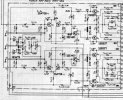
Note: I have attached a part of the schematic.


1-
I have verified that the preamplifier stage delivers an AC signal with no DC component. With this I have ruled out a problem in this stage and whatever is generating the DC Offset is further down the chain.

2-
My first suspect was the 2SA798 differential transistor, so I fabricated two new ones using 2xKSA992FTA. To match them I used this "digital transistor tester", I know it's not the best method but I guess it's good enough to see an improvement. But it didn't change anything.

3-
I have measured voltages in the amplifier stage and now in addition to values related to DC Offset, it also appears that the bases of the power transistors are not receiving the +/- 1.2 volts that the manufacturer states, but +/- 0.6v. In the following tables you can see the results of the measurements.

Differential TransistorsB1C1EC2B2
Should be0-47.6-0.6-47.60
Q3 [V] (Left)0.076-45.10.65-45.70.087
Q4 [V] (Right)0.084-450.66-45.90.095

Driver TransistorsBCE
should be [V]+/- 1.2+/- 1.2
Q9 [V] (PNP Left)-1.2-41.6-0.6
Q11 [V] (NPN Left)1.241.50.6
Q10 [V] (PNP Right)-1.2-41.7-0.6
Q12 [V] (NPN Right)1.241.60.6

Output TransistorsBCE
should be [V]+/- 1.2+/- 40+/- 0.6
Q13 [V] (PNP Left)-0.6-420.02
Q15 [V] (NPN Left)0.65420.06
Q14 [V] (PNP Right)-0.56-420.03
Q16 [V] (NPN Right)0.65420.06

4-
At this point I began to doubt my previous repair and so I removed the output transistors and measured once again. All voltages remain unchanged.
NOTE: All of the following steps I have executed without reassembling these transistors.

5-
I have measured the emitter resistors (R57 to RR60) and all the 1/2 watt resistors around the output transistors and drivers. All resistors showed the values indicated by the manufacturer (R49 to R52 150ohm and R53 to R56 4.7ohm).

6-
I have replaced the drivers using Toshiba tta004b-q/ttc004b-q, as closely matched as possible. But the voltages remain as before.

7-
I have replaced D1 to D6. For diodes D1-D4 I used 1N4148 and for D3-D4 I found a reputable seller on eBay. After these changes, the voltages remain unchanged.

8-
I removed the protective relay, just to try something different, but the voltages remain unchanged.

Help !!!
As you can see, I have tried many things and the problem persists.
Is the DC Offset related to the discrepancy in the base of the power transistors? Are they separate problems?
What can you recommend to identify the cause of these problems?

Thank you very much in advance and I wish you a very good day :)
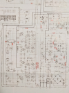
 

Attachments

  • Schematic.png
    Schematic.png
    909.9 KB · Views: 10
Register to hide this ad
Hi guys,

As the title says, the amp has DC Offset and I don't know the cause, so I'm publishing this post, hoping that someone can help me, because I've run out of ideas (also quite frustrated :/ )

A little context ...
I have had this pioneer sa-7500ii for a few months now and it originally had the right channel output transistors and the diodes of the rectifier stage damaged.
I replaced the output transistors using these Toshiba 2sa1943n/2sc5200n (recommended by @markthefixer and they work perfect) and these RGP30M-E3/54 diodes for the rectifier stage. I have also replaced all the resistors in the power amplifier stage that should dissipate 1/2W or more with new Metal Oxide resistors.
With these changes the amplifier was up and running again. Therefore I have started to replace the electrolytic capacitors, using this restoration guide.
Once finished, I measured bias, DC offset and output signal (with an oscilloscope). All measurements were within the manufacturer's specifications, only the left channel bias measurement was a little high (56mV) but still below the 70mV indicated by the manufacturer in the service manual. And the sound test was very satisfactory, the amp was fixed and sounded very good in my opinion.

After using it for a couple of months I noticed a little “pop” when turning off the amplifier, so once again I opened it to measure voltages in the protection stage. But before that I measured again bias and DC offset and here something new appeared. Now both channels had around 50mV as DC offset. Here are the exact measurements.
LeftRight
DC offset [mV]4056
Bias [mV] (ok between 10 and 70)5339

The following sequence shows what I have tried so far, in time order, to solve or identify the problem (no success so far).
Note: I have attached a part of the schematic.


1-
I have verified that the preamplifier stage delivers an AC signal with no DC component. With this I have ruled out a problem in this stage and whatever is generating the DC Offset is further down the chain.

2-
My first suspect was the 2SA798 differential transistor, so I fabricated two new ones using 2xKSA992FTA. To match them I used this "digital transistor tester", I know it's not the best method but I guess it's good enough to see an improvement. But it didn't change anything.

3-
I have measured voltages in the amplifier stage and now in addition to values related to DC Offset, it also appears that the bases of the power transistors are not receiving the +/- 1.2 volts that the manufacturer states, but +/- 0.6v. In the following tables you can see the results of the measurements.

Differential TransistorsB1C1EC2B2
Should be0-47.6-0.6-47.60
Q3 [V] (Left)0.076-45.10.65-45.70.087
Q4 [V] (Right)0.084-450.66-45.90.095

Driver TransistorsBCE
should be [V]+/- 1.2+/- 1.2
Q9 [V] (PNP Left)-1.2-41.6-0.6
Q11 [V] (NPN Left)1.241.50.6
Q10 [V] (PNP Right)-1.2-41.7-0.6
Q12 [V] (NPN Right)1.241.60.6

Output TransistorsBCE
should be [V]+/- 1.2+/- 40+/- 0.6
Q13 [V] (PNP Left)-0.6-420.02
Q15 [V] (NPN Left)0.65420.06
Q14 [V] (PNP Right)-0.56-420.03
Q16 [V] (NPN Right)0.65420.06

4-
At this point I began to doubt my previous repair and so I removed the output transistors and measured once again. All voltages remain unchanged.
NOTE: All of the following steps I have executed without reassembling these transistors.

5-
I have measured the emitter resistors (R57 to RR60) and all the 1/2 watt resistors around the output transistors and drivers. All resistors showed the values indicated by the manufacturer (R49 to R52 150ohm and R53 to R56 4.7ohm).

6-
I have replaced the drivers using Toshiba tta004b-q/ttc004b-q, as closely matched as possible. But the voltages remain as before.

7-
I have replaced D1 to D6. For diodes D1-D4 I used 1N4148 and for D3-D4 I found a reputable seller on eBay. After these changes, the voltages remain unchanged.

8-
I removed the protective relay, just to try something different, but the voltages remain unchanged.

Help !!!
As you can see, I have tried many things and the problem persists.
Is the DC Offset related to the discrepancy in the base of the power transistors? Are they separate problems?
What can you recommend to identify the cause of these problems?

Thank you very much in advance and I wish you a very good day :)

You already tried the diff amp pairs which is usually the culprit. Those cheap little testers can be good enough if they are consistent. One thing to be aware of is that just by holding the transistor between your fingers while you put in the tester your body heat can dramatically alter the readings. Try it, load a transistor, measure it then pinch it between your fingers for 10 seconds and measure again. I always use tweezers to handle them for matching.
 
Last edited:
You already tried the diff amp pairs which is usually the culprit. Those cheap little testers can be good enough if they are consistent. One thing to be aware of is that just by holding the transistor between your fingers while you put in the tester your body heat can dramatically alter the readings. Try it, load a transistor, measure it then pinch it between your fingers for 10 seconds and measure again. I always use tweezers to handle them for matching.
Hi @mrk229

thanks for your reply. In fact I did use a tweezer to handle them.
The matching procedure was the following ...
- left all transistor over the same surface for at least one hour, so all got the room temperature.
- with tweezers took the legs and insert the transistor to measure it. I did measure them fast and one after the other. I put them over a sheet with the measurements.
- after 30 minutes came back and did measure them again. Once again, I did put them over the sheet with the old values.
- after another 30 minutes I have repeated the measurements

With the selected pairs.
- I used thermal glue to join them (flat face with flat face) and did let them alone under "pressure" for one hour.
- to avoid undesired short-circuits between the legs, I covered them with heatshrink tubing
- finally I wrapped the transistors with heatshrink

I think I did a good work, but who knows hahahahaha

What is interesting, is that the DC-Offset didn't change. It was maybe just a couple of mV less but nothing like 10mV or 15mV in one or the other direction that did make a statement ... like, yes ... here is the problem :/

So ... here I am... I've run out of ideas. Maybe I can ask someone to build them and sell them to me.

Have a nice day and thanks again for your time :)
 
Sounds like you did everything right. Perhaps with the simplification of the circuit which has no real adjustments it is the best it can be? The SA-7500 series one has both offset and bias adjustments.

Where did you come up with the base drive for the outputs being + and - 1.2 volts?
 
Sounds like you did everything right. Perhaps with the simplification of the circuit which has no real adjustments it is the best it can be? The SA-7500 series one has both offset and bias adjustments.

Where did you come up with the base drive for the outputs being + and - 1.2 volts?
Hi @mrk229

The first time I did repair it, the DC Offset was under 10mV for each channel. So I know it can be better, but as you say without an adjust mechanism is hard to find what could be "wrong". I know 50mV isn't "that bad", but the change is what makes me worry, maybe now I say ... "well, it is what it is" and three months later is up again to 100mV and a year later 300mV and so on. I'd prefer to avoid that situation and fix it now for good.

The voltages for the output power transistors are found in the service manual (please see the attached picture Q13/Q15). That is the only place where those are found, but I have found at least one error related to voltages in the service manual, and it was for Q3 and Q4 (the differential transistors), where in one diagram they say the emitters should have -0.6V and in the next pages the value is 0.6V ... so, I can't be 100% sure about it.

What really worries me is the DC Offset that may in the future damage the speakers, the voltages at the bases of the power transistors may be a symptom or perhaps a mistake in the service manual. However, without DC Offset and the amplifier, amplifying correctly and measuring a bias current within the range specified by the manufacturer, it would be enough for me and I would have peace of mind.

Thanks again and have a nice day.
 

Attachments

  • Output_Power_Transistors.png
    Output_Power_Transistors.png
    1,002.2 KB · Views: 3
I would humbly suggest that voltage is an error. The base drive on the driver would be 1.2 or -1.2 and then the EB drop through the drive would leave .6 or -.6 base voltage on the outputs resulting in + or - zero after the output EB drop. Pretty sure the diagram is wrong. I understand the concern about excess offset but the protection circuit should prevent any damage to the speakers by opening the relay.

That said if it was lower before then certainly something has changed. Have you checked the power supply voltages that feed the diff amp?

7500ps.jpg
 
Saw this in the "similar threads" box. Some additional info, but no real solution.
 
I would humbly suggest that voltage is an error. The base drive on the driver would be 1.2 or -1.2 and then the EB drop through the drive would leave .6 or -.6 base voltage on the outputs resulting in + or - zero after the output EB drop. Pretty sure the diagram is wrong. I understand the concern about excess offset but the protection circuit should prevent any damage to the speakers by opening the relay.

That said if it was lower before then certainly something has changed. Have you checked the power supply voltages that feed the diff amp?

View attachment 3376668
Hi @mrk229

Thanks for you analyze of base voltages on the output transistors, and it make sense :)

The power supply voltages:
- At the emitters of Q7 and Q8 I have 41.2V as the service manual says. So between the remitter resistors R43 and R44 must be 42.4V
- At the emitters of Q5 and Q6 the voltage is little lower, it should be -47.6V and I have -46.3V. Yesterday I went to that path and found that the resistor R97 was toasted, it marked 270ohm but I changed anyways. I didn't have a 270ohm resistor, but I made one with 1x150ohm (metal oxide 1W) in series with 4x470ohm/1/4W in parallel, the final "Frankenstein" resistor measured 267ohm, so ... close enough. I could play with that resistor to have the expected -47.6V, but I am not sure it will change the DC offset, but maybe I'm wrong.

Thanks !!!
 
Saw this in the "similar threads" box. Some additional info, but no real solution.
Yeah ... the OP had to play with the hfe of the differentials and drivers. It's all very tight and sadly the "cheap" design do not provide any adjustment. I'm thinkin (just for fun), to copy the sa-7500 circuit to adjust the dc offset, but every service manual that I have found in internet is very blurry and I do not have an HiFi-Engine account (I can't make one, they do not accept new users), maybe that version has a better resolution. @mrk229 could you perhaps obtain it and share it?
If I go down that road and have success ... then next could play a bit with the bias adjust. if I replace R45 and R47 for a variable 20ohm resistor, maybe it gave a bit of adjust.
This is beautiful amp and I do not plan to sell it, so I don't really care much if I do some changes. I don't want to make an abomination of it, but if I can tweak those two thinks would be great.
 
Yeah ... the OP had to play with the hfe of the differentials and drivers. It's all very tight and sadly the "cheap" design do not provide any adjustment. I'm thinkin (just for fun), to copy the sa-7500 circuit to adjust the dc offset, but every service manual that I have found in internet is very blurry and I do not have an HiFi-Engine account (I can't make one, they do not accept new users), maybe that version has a better resolution. @mrk229 could you perhaps obtain it and share it?
If I go down that road and have success ... then next could play a bit with the bias adjust. if I replace R45 and R47 for a variable 20ohm resistor, maybe it gave a bit of adjust.
This is beautiful amp and I do not plan to sell it, so I don't really care much if I do some changes. I don't want to make an abomination of it, but if I can tweak those two thinks would be great.
I have the HFE service manual, but it's too large to post or message in AK.

Here's the scat from HFE:
 

Attachments

Last edited:
I think you can get what you need from this. If not I can e-mail you the original file which is too large to post here.

7500MKI.jpg
 
I think you can get what you need from this. If not I can e-mail you the original file which is too large to post here.

View attachment 3378157
Hi @mrk229

that's exactly what I needed !!!!. Anyway @satellite65 has already sent me the service manual by email.
You guys are just great, thank you very much for the support.

I think I know how to put the two circuits together and the -13V voltage will be taken from a -20V voltage I found on the motherboard and a resistive divider. I will try to find time this week to design a PCB and send it to build.
I will let you know as soon as I have any news.

Thanks again and I wish you a nice holidays.
 
Hi @mrk229 , hi @satellite65

I have simulated the circuit and it works, but the C19 and C20 "explodes" ... So I checked again the sa-7500 service manual (Power Amplifier Assembly AWH-040) and those caps are in the schematic but not in the component list. I think, I won't use them and see what happens. Still will design the PCB having them in case they will be needed.

Now I have to design the PCB and when I know the dimensions, then I will analyze where there is a space inside the amplifier to install it. But I figure I can use a 3D printer to design a base that will be “glued” to the motherboard and into which the board can be inserted vertically. That way, the changes I make can be reversed if desired.

The only thing that bothers me is having to place an order at Mouser or Digi key for a few resistors and potentiometers, and having to pay more for shipping than for the components :rolleyes:

Have a nice day :)
 
Hi @mrk229 , hi @satellite65

I have simulated the circuit and it works, but the C19 and C20 "explodes" ... So I checked again the sa-7500 service manual (Power Amplifier Assembly AWH-040) and those caps are in the schematic but not in the component list. I think, I won't use them and see what happens. Still will design the PCB having them in case they will be needed.

Now I have to design the PCB and when I know the dimensions, then I will analyze where there is a space inside the amplifier to install it. But I figure I can use a 3D printer to design a base that will be “glued” to the motherboard and into which the board can be inserted vertically. That way, the changes I make can be reversed if desired.

The only thing that bothers me is having to place an order at Mouser or Digi key for a few resistors and potentiometers, and having to pay more for shipping than for the components :rolleyes:

Have a nice day :)
Caps usually blow up for two reasons. Reverse polarity or over voltage. They are electrically on the wipers (output) of the pots to ground. Oddly looking at the circuit they could see a small reverse voltage depending on the setting of the pot. Even then I don't think there can be enough current to make them explode?

I can always find something to stock up on to "plus" up an order. I seem to always need another speaker protection relay or two.
 
Back
Top Bottom