• The move to the new server is done. There are some software and database maintenance updates in process. This has us passing the hat around to help out. We appreciate any donations. Seriously, even a dollar helps. The payment page may be found here - https://www.audiokarma.org/support.html

Pioneer sx-737 bias issue max 1mV in one channel

Cichoslav

Member
Hello, I found some really valuable info and help here, but I suppose it's time to start my own thread. I'm stuck for 3 days straight and frustrated to the moon.

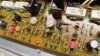
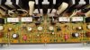
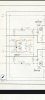
I got a SX-737 unit with fried transformer (secondary for full wave rectifier, pins 3&4 on the ps board). It's repaired now, but I spotted an issue with bias regulation on power amp board

Left channel - all good. Bias can be adjusted, dc offset too. Voltages on output transistors bases ca. 0.54V

Right channel - can't adjust bias. It regulates between 0-1.1mV.
I changed spv4 to 4x 1n4148 and it widened the range to 3mV

I changed outputs with left channel, no change. Issue stayed it the right. I have +34V and - 34V on filter caps.

Voltage on bad channel output bases vary depending on dc offset - when they're comparable, dc offset is like 80mV or so. Whe offset is set to 0, one base is below 0.5V, other one reaches around 0.65V

I am aware of the idle/offset error in SM

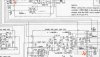
I swapped all 2sa726 and 2sc1451 transistors on the power amp board with recommended ksc's and bd139/140 as drivers, changed Sanyo capsistors to wima foil caps, changed electrolytes, measured 150r, 4r7 and 0r5 resistors, even followed and compared resistor values with SM - pcb looked all original, but there are resistors that don't match with values. So - there should be 3.4V and -3.4V after R39 and R40, I'm getting 0.7V and -1.5V

Resistor No. / installed value / SM value

R39 30k 56k
R40 20k 18k
R41 680r 6.8k
R42 1.8k 5.6k
R43 10k 56k
R44 22k 51k

All of the above were one-leg lifted and measured good.

Voltages on pin 6 and 10 are spot on. 35V and -13V
Grounds are good
Trimpots cleaned and measured good - 100r and 10k

Basically all parts I replaced measured good and replacing them with new substitutes didn't change a thing.

Let me know what info do you need me to provide and I'll do it. Just please help me.
 

Attachments

  • Screenshot_2023-05-29-19-18-23-624_com.google.android.apps.docs.jpg
    Screenshot_2023-05-29-19-18-23-624_com.google.android.apps.docs.jpg
    61 KB · Views: 15
  • Screenshot_2023-05-27-17-01-34-165_com.google.android.apps.docs.jpg
    Screenshot_2023-05-27-17-01-34-165_com.google.android.apps.docs.jpg
    70.7 KB · Views: 17
  • IMG_20230530_191103.jpg
    IMG_20230530_191103.jpg
    99.1 KB · Views: 20
  • IMG_20230529_203612.jpg
    IMG_20230529_203612.jpg
    103.9 KB · Views: 17
Register to hide this ad
is the prestage -B, -40v present?
R22 value?
1451’s with 3503’s?
Curious. Was this an issue before you tinkered with it?
Check the emitter resistors for value.

I would have checked all the resistors and diodes on that amp channel.
Checked all the supply voltages.
Rechecked all my soldering and polarized components for correct placement.
I don’t trust my self. Well, maybe one percent of the time. That’s why you have to have a process and double check yourself. Me anyway.
 
Last edited:
Hi, Thank you for your response.

B- is present, but a pinch lower than -40V. Around -37V. I'll check it for sure when I get back home form work.

I omitted lifting the r22 leg, in circuit it was 100ohm, I'll check it today with one leg lifted as well as the others I left.

Emitter resistors are fine, I shorted my meter leads so I knew the "zero", they're 0,55 and 0.52ohms.
There are 3 diodes - two stv4's that work fine and the d3 I replaced already. I always double check for transistors, as those are tricky and their legs are mixed up most of the time. I use t4 transistor tester that shows symbol, polarity and determines what is what. Then I take a pic and mount them according to the print on the board.

Yes, it was an issue from the very beginning since I turned it on for the first time after transformer and supply fix. I thought this will be enough, but I was wrong. Also there's no relay click, but I suppose it's another issue for another time.

This one gives me a serious headache. I suppose there's one faulty element there and I cannot find it. Output transistors are tested and working, so that's not it. Also I don't understand where's that -40V coming from. Maybe that's the issue here? Good point with mentioning that one.

Greetings from Poland.


Edit: found it. So it's not exactly -40V. Image below
 

Attachments

  • Screenshot_2023-05-31-15-02-02-138_com.google.android.apps.docs-edit.jpg
    Screenshot_2023-05-31-15-02-02-138_com.google.android.apps.docs-edit.jpg
    107.7 KB · Views: 16
Last edited:
You might know this already:
When turning the trimmer to increase the bias your increasing the circuit resistance between the drivers.
I have to think about that when I'm troubleshooting it.
Base voltages at Q7,Q8?
The 37v is low but so are the rails. That's not an issue.
 
Last edited:
There is a B+ for the pre stage too.
I’m at work and looking at this between jobs.
Look for those expected “B” voltages and look for broken traces. It may of been dropped?
 
No worries, we all have our lives and responsibilities.

Made some measurements, lifted and checked rest of the resistors I previously skipped

R2 24.6k
R8 49.4k
R12 1.79k
R14 1.19k
R16 24.6k
R20 3.97k
R22 100.5R
R24 148.4R
R26 150R
R28 4.7R
R30 4.7R

Voltages measured on each pin of the power amp board to chassis GND

1. -2mV
2. 3mV
3. 0mv, +-2mv fluctuating
4. 0V
5. 0V
6. 35.5V
7. 0V
8. 0V
9. -36.3V
10. -13.5V
11. 0V
12. -36.5V
13. -36.5V
14. 0V
15. 0V
16. 0V
17. 0.2mV fluctuating
18. - 0.1mV
19. - 0.1mV
20. - 0.1mV
21. 0.53V
22. 36.5V
23. -1.5mV
24. -0.48V
25. -36.5V
26. -5mV
27. -0.53V
28. -36.3V
29. - 36.3V
30. 3mV
31. 0.55V
32. 36.4V
33. 36.4V

Voltages measured Q base-GND:
Q7 1.17V
Q8 -1.14V
Q9 1.15V
Q10 - 1.09V
 
Can you recheck the Voltages measured Q base-GND:
Q7 1.17V, looks good
Q8 -1.14V, should be positive
Q9 1.15V, should be negative
Q10 - 1.09V, is negative, looks good
 
Q7 1.17V
Q8 1.14V
Q9 -1.15V
Q10 - 1.09V


You're right. My bad. Rechecked.


Also used an audio probe. There is audio on both outputs. Just can't set the bias on one of them. Even used different meter to double check if it's there or not.
 
Last edited:
I have examined the thread carefully.

Your readings show 8 milliamps idle current on the left channel, minimal milliamps on the right channel.

Test #1: CAREFULLY trade D1 & D2, the STV-4h's. recheck which channel (or both) sets, or which doesn't.
post Q7 through Q10 base & EMITTER voltages.
post voltage across vr1, across vr2 and idle currents.
with power off, measure and post the Ω resistance of VR1, and then measure and post the Ω resistance of VR2.

some explanations:

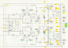
C9(C10) 47uf / 35v is the "bootstrap" capacitor. It is charged to +35v through R11 (R12)
it's negative is connected to the output of the amp - which is normally about 0 volts.
The bootstrap capacitor's charge flows out through R19 (R20) as a nominally steady current.
When audio comes through it raises the capacitor's negative terminal voltage, and the positive terminal follows PLUS it's 35v charge.
Always ensuring that the R19 (R20) current stays the same.

what's so important about this current?

The current flows through the STV diode(s) to get a specific voltage at a specific temperature.
If the current increases or decreases, the voltage provided by the STV diode(S) increases or decreases - IRRESPECTIVE of ANY temperature difference.

Then the VAS transistor Q5 (Q6) gets it's conductance varied (by Q2 / Q4 input stage) so that the output balances the input, and the STV voltages show up as +1.2v and -1.2v at the bases of the drivers.

From what I can see, your STV diodes are delivering 2.32 volts on the settable channel and 2.23 volts on the non-settable channel.

This lower voltage of that STV can be either a characteristic of that part, OR an indicator that the current through the diode is low.

Swapping them would answer some questions.

It could be that on this circuit, all the tolerance variations allowable all stacked up on the wrong side of each's curve.

The drivers seem ok, they have Vbe's of : 0.6345, 0.62, 0.61 & 0.61.

0.61 & 0.61. are on the non-settable channel.- so they may be teetering on the edge of working.

A comparison of R19 & R20 values might be instructive.


upload_2023-5-31_20-19-57.png
 
Last edited:
Thanks Mark.

I'll measure, trade and post results as soon as I can. I forgot to mention I changed to bd139/bd140 only Q8 and Q10. Left the old oem drivers in left channel. I can change Q7 and Q9 too if necessary for more uniform comparison.

I'll lift R19 and measure resistance, as we already have R20 measured and listed
Measure B-E voltages Q7 to Q10 respectively,

Across VR1 and VR2 meaning i measure voltage drop on vr's and put my meter leads between STV4H anode and Q7(Q8) base?
Also i don't want to tweak and turn the VR1 because of its functionality and risk of setting too high bias, I'll measure it as is. It is just set to low, just in case.
I'll check the VR2 on min and max though, because there's only 1.1mV bias when fully turned to the right.

Also idle current - where do I have to connect my meter clips? As I'm aware I have to desolder one leg of a specific component and plug my meter there in series.

I apologize in advance for newbie questions, but better safe than sorry.

Measuring those may take a while, as I have to read in English and translate my thoughts to polish. Thank you for your reply and deep analysis of the problem. I was silently hoping for your response.


Edit: I'll try to change electrolytic capacitors on the power supply board. I left them as they were, but it came to me, that there was some sort of a problem and two hot spots. There are four el caps next to 180R 5W and 2SD313 stabilizer. This operation wouldn't make any harm.
 
Last edited:
Your new driver transistors on the right channel need just a little more voltage (Vbe) than the ones on the left channel. The solution is very simple. Add a small resistor in series with D2. A resistor of 10 Ohm should be enough.
 
Okay, I took some measurements

Vr1 and vr2 are both adjustable within 0 to 86 ohms range.

When bias set to 3mV in left, Vr1 shows 0.075V voltage drop between leads.

When bias set to 0.5mV in right, (like middle of the pot) Vr2 shows 0.252mV voltage drop between leads.

B-E voltages with this settings are:

Q8 0.624v
Q10 -0.621v
Q9 -0.618v
Q7. 0.628v

Q11 0.532v
Q13 -0.512v
Q14 -0.515v
Q12 0.708v


When Vr1 and vr2 are set to 15 ohms, there's 87/86mV voltage drop on both.

In this case both stv4h's voltage drop between leads is 2.21V

B-E voltages measured with this particular vr1&2 settings are:

Q7. 0.623v
Q9. - 0.595v
Q8. 0.626v
Q10. - 0.617v

Q11. 0.539v
Q13. -0.520v
Q14. -0.490v
Q12. 0.573v

In both cases dc offset was set to 0v

Missing resistors measurements:

R4 2.2k
R6 83.1k
R10 4.4k

R19 3.94k
 
I have not analyzed the latest numbers, yet. because:

This struck me:
I forgot to mention I changed to bd139/bd140 only Q8 and Q10. Left the old oem drivers in left channel. I can change Q7 and Q9 too if necessary for more uniform comparison.

It is the root of the problem. The channel with the old drivers adjusts. The non-adjustable channel has the new drivers.

ecluser smacks the problem right on the nose. Do as he says. I might swap the pots out for new 200 ohm pots. All the adjustment range you might need.
 
Oh I'm sorry, I can put back the old drivers, as they appeared to be just fine. Changed them to BD's anyway, because I'm trying every possible way to find and somehow blindfolded solve that problem, but replacing them didn't make any change. My experience with electronics is very low, just rebuilding things from scratch following schematics and building guitar pedals with given BOM and pcb layouts. Troubleshooting isn't my piece of cake yet.
 
Last edited:
I might swap the pots out for new 200 ohm pots. All the adjustment range you might need.

I fear that with 200 Ohm trim pot, the bias adjustment would be oversensitive.

Can you confirm that you have the correct voltages at the collectors of the power transistors in the right channel? I know that you have the correct voltages at pins 22, 25, 28 and 33. Make sure there is good electrical contact with the case (collector).

Beware that in some amplifiers you might need to turn the bias trim pot clockwise in one channel, and counter-clockwise in the other channel, in order to increase the bias. I can not say if the SX-737 is like that, but check to be sure that you are turning the bias in the good direction on the right channel.
 
I would get the amps up, stable and running first.
Protection might operate correctly.
 
@markthefixer, Just a thought, what about a full check on the protection board and solving this issue first? Or is that related to the unstable bias voltage?


I suppose it's bias related. Spent whole evening changing caps, diodes and transistors with no luck at all. I noticed I'm like missing 1V somewhere. Between Q5 and Q6 on the protection board I should have -1V, where I have 0. Checked resistors in that area and everything works just fine. Relay coil is working, Checked with ext power supply. In my opinion protection circuit is working correctly.


Edit: swapped vr2 with 220R.
I could set bias to 3.8mV max in this configuration.


Q12 B-E -0.56V
Q14 B-E 1.75V

I am going to change emitter resistors just in case and mount the original 100R pot back.
 
Last edited:
Q14 B-E 1.75V????

That transistor is bad.


Is it possible that transistor tests good with a tester and multimetr and starts to act up when under load? I'm a newbie and lack experience.

Also I packed it and sent to a more experieced technician. This one overwhelmed me and I gave up. I'll post the solution as soon as it's fixed and I get some info.
 
Last edited:
Back
Top Bottom