

You are using an out of date browser. It may not display this or other websites correctly.
You should upgrade or use an alternative browser.
You should upgrade or use an alternative browser.
Pioneer SX-737 No Sound, No Relay Click, Lights On
- Thread starter golfnut
- Start date
-
- Tags
- pioneer 737
Habit I guess.I always wonder, why you don’t stick the parts direct into the Universal-ZIF-Socket

gslikker
Super Member
No, R10 disconnected or not should not influence it, because the 35V is (read: should be) regulated. R10 lifted just disconnects equalizer amp power for the moment and should make troubleshooting easier.@gslikker I agree with you, that the voltage difference of 1.5 Volt between B and E on Q1 is too high, and strange as well the voltage difference of 0.1 Volt between B and E on Q2 is too low.
BUT could that be caused by the disconnected R10, to keep the Equalizer Amplifier Assembly AWF-011 isolated?
How would you proceed from here?
My next step would be some test on the protection board.
More test on the power amp to get pin 1 and 3 sorted out
In between if time permits, solving the issue on the AWF-011
Thoughts?
Now, the 33.5 Volts could be correct if the base of Q2 is 14 Volts as indicated in post 474
In that case, 33V-something on the supply output is right.
But at the same time measurement states the emitter of Q2 to be 14.1 Volts.
This is the zener diode voltage, which is correct and as expected.
So, there is something really wrong there, since if the zener diode voltage is 14.1, then the base of Q2 SHOULD be between 14.6 and 15.
Just look at the figures what to measure in the schematic on page 54.
I have seen too much different measurements now, there is no way for me to conclude anything.
My own conclusion at the moment can only be that for now I see two different things which are NOT normal in the post 474 readings on the Q1/Q2 transistors, and they can NOT be explained the way it is measured in the regulating circuit now.
In such case, myself I always use the oscilloscope to see what is going on, but for now myself I am stuck here, so I am out of ideas.
Last edited:
I don't know if this helps but I just took new measurements. This was after replacing a transistor Q7 on the 025 board. 2SC1384 was replaced with KSC2690. The 1384 npn measured at 623 and 626.No, R10 disconnected or not should not influence it, because the 35V is (read: should be) regulated. R10 lifted just disconnects equalizer amp power for the moment and should make troubleshooting easier.
Now, the 33.5 Volts could be correct if the base of Q2 is 14 Volts as indicated in post 474
In that case, 33V-something on the supply output is right.
But at the same time measurement states the emitter of Q2 to be 14.1 Volts.
This is the zener diode voltage, which is correct and as expected.
So, there is something really wrong there, since if the zener diode voltage is 14.1, then the base of Q2 SHOULD be between 14.6 and 15.
Just look at the figures what to measure in the schematic on page 54.
I have seen too much different measurements now, there is no way for me to conclude anything.
My own conclusion at the moment can only be that for now I see two different things which are NOT normal in the post 474 readings on the Q1/Q2 transistors, and they can NOT be explained the way it is measured in the regulating circuit now.
In such case, myself I always use the oscilloscope to see what is going on, but for now myself I am stuck here, so I am out of ideas.
From post 474
Q1/B/C/E
35.0/48.0/33.7
Q2/B/C/E
14.0/35.0/14.1
Readings now:
Q1/B/C/E
34.9/47.6/33.8
Q2/B/C/E
14.0/34.8/13.9
Zener Diode
0/13.8
Your measurements are a real problem and lead to confusion.
Just one example from post #486 regarding the voltage of all three diodes D5-7.
I asked on purpose for the anode voltage for all three, knowing that they are all on the same trace and should be pretty close.
Your note on the layout shows THREE different measurements. If I read it correctly, you have at anode D5 11-16V, at D7 17.1 and at D6 18.1volt. That’s a spread from 11 to 18.1 volt all on the same trace!
To avoid confusion like that, I never use auto range on my audio units.
Hopefully, this puzzle with the fluctuating values can be explained someday.
Attachments

What should they measure? Mine seem to jump around with no constant measure even with a different dmm.Your measurements are a real problem and lead to confusion.
Just one example from post #486 regarding the voltage of all three diodes D5-7.
I asked on purpose for the anode voltage for all three, knowing that they are all on the same trace and should be pretty close.
Your note on the layout shows THREE different measurements. If I read it correctly, you have at anode D5 11-16V, at D7 17.1 and at D6 18.1volt. That’s a spread from 11 to 18.1 volt all on the same trace!
To avoid confusion like that, I never use auto range on my audio units.
Hopefully, this puzzle with the fluctuating values can be explained someday.
The R18, 20 and 22 I do get a constant 34.1vdc on the same trace.
Well I’m not getting any way near that. I just turned it on and all 3 points were 2.6vdc. Then they’ll all jump up to around 4vdc. Then up to around 12vdv. Then settle back down. If they are to be constant, these are not.They should be around 20 vdc.
Regarding the protection board, I have replaced the 1384 with 2690. I do not have the other transistors to replace. I’ve attached a picture of the transistors I have.Can you provide a focused picture from the solder said. Maybe there are some bad solder joints in the area of D5-7.
What to your plan next on the protection board?
I bought these when I was working on another unit some time ago.
Here’s the picture of foil side of 025.
Attachments


Let’s assume that your DMM works fine and constant 34.1vdc for R18, 20 and 22 is in line with the vdc at pin 10 and 11. Should be the same like at R13 and 14 on the same trace.
The fluctuating measurements at the diodes are a real problem and may point to a dying Q5.
What I would suggest next. Wait for the new parts to arrive and replace Q1-2 and Q6 as well. In the mean time you can pull Q5 and test it, but if it’s already out, I would replace Q5 as well. After that, test the vdc at D5-7, Q5, Q6 and Q7 again.
The recommended replacement parts are:
Q5 with KSA992 and Q6 with KSC2383YTA
If there is still no stable relay click, we have to check some caps.
Right now, Q3 and Q4 appear to be good.
Last edited:
I will be very busy for the next 6 days and won’t be online as usual. Just replace the parts und take care. Now you should be used to take controlling measurement after you change parts. When finish with the AWF-011 you can reconnect the R10 again, and as before check the voltage on the power supply pin 14, 15 and 17.
I should have my replacement parts by then. Thanks and we'll chat later.I will be very busy for the next 6 days and won’t be online as usual. Just replace the parts und take care. Now you should be used to take controlling measurement after you change parts. When finish with the AWF-011 you can reconnect the R10 again, and as before check the voltage on the power supply pin 14, 15 and 17.
Apparently Digikey was a few days behind shipping so they are scheduled to arrive Monday, March 2.I’m still waiting on the parts to arrive.
AWM-025 update with new transistors.Let’s assume that your DMM works fine and constant 34.1vdc for R18, 20 and 22 is in line with the vdc at pin 10 and 11. Should be the same like at R13 and 14 on the same trace.
The fluctuating measurements at the diodes are a real problem and may point to a dying Q5.
What I would suggest next. Wait for the new parts to arrive and replace Q1-2 and Q6 as well. In the mean time you can pull Q5 and test it, but if it’s already out, I would replace Q5 as well. After that, test the vdc at D5-7, Q5, Q6 and Q7 again.
The recommended replacement parts are:
Q5 with KSA992 and Q6 with KSC2383YTA
If there is still no stable relay click, we have to check some caps.
Right now, Q3 and Q4 appear to be good.
Q1 Q2 were removed with ksc2383
Q3,Q4,Q6 were replaced with ksc945
Q5 was replaced with ksa992
Q7 was replaced with ksc2690
Continuity was checked.
D5,D6,D7 all measured 9.5vdc (not the 20vdc we expected)
Transistor measurements were also off.
Q/E/C/B vdc
7/0/33.9/0
5/10/.7/9.3
6/0/0/.6
I obviously have no relay click.
I have not attached the R10 leg.
Picture of the board are attached.
Attachments


Last edited:

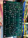
After the above changes on the 011 and 025 boards and reattaching the R10 resistor leg on the PS board, I took new PS board measurements. Unit was on full power. The relay did not click off so still in protection. Just about every measurement increased in voltage including the pin17 which has been somewhat of a problem.
Should I begin changing out the caps? The only caps I have changed is on the PS board and all the blue tantalums. The blue ones were changed with e-caps and not the other types. If I'm to change caps, would the amp board be the first one to tackle?
| Pin | Measured Voltage | Expected Voltage if known |
| 1 | 7.9 | 7.5-8 vac |
| 2 | 7.7 | 7.5-8 vac |
| 3 | 39 | |
| 4 | 39 | |
| 6 | 37.1 | |
| 8 | 27 | |
| 11 | 27.1 | |
| pin to pin measurements, remove black lead from chassis and use red and black for pin to pin | ||
| Pin 3 to pin 4 | 78.2 | |
| Pin 8 to pin 11 | 54 |
| Pin | Measured voltage | Expected voltage if known |
| 7 | -38.5 | -36 vdc |
| 9 | 36.1 | +37vdc |
| 10 | -35.8 | -37vdc |
| 12 | -13.3 | -13vdc |
| 13 | -13.3 | -13vdc |
| 14 | 34.1 | +36vdc |
| 15 | 30.7 | +31.5vdc |
| 16 | 30.7 | +31.5vdc |
| 17 | 26 | +24vdc |
| 19 | 12.9 | +13.5vdc |
| 20 | 12.9 | +13.5vdc |
| 21 | 5.9 on aux; 12.9 on AM | +13.5vdc |
Should I begin changing out the caps? The only caps I have changed is on the PS board and all the blue tantalums. The blue ones were changed with e-caps and not the other types. If I'm to change caps, would the amp board be the first one to tackle?
Welcome back,
your measurement don’t lock good and there are still some issues on the protection board.
Let’s first concentrate on the protection AWM_025.
The greatest problem with your picture, there is too much shadow and the transistor pins are concealed by the component.
I compared the transistors from your picture with my board, and I’m not sure if Q3, Q4, Q6 and Q7 are installed correct.
Please recheck your transistor pin out with my picture and if you are certain, that they are installed correct, post pictures from all 4 transistors showing the front side and the pins, preferably without shadows or board print hidden from others parts.
Glad to be back!Welcome back,
your measurement don’t lock good and there are still some issues on the protection board.
Let’s first concentrate on the protection AWM_025.
The greatest problem with your picture, there is too much shadow and the transistor pins are concealed by the component.
I compared the transistors from your picture with my board, and I’m not sure if Q3, Q4, Q6 and Q7 are installed correct.
Please recheck your transistor pin out with my picture and if you are certain, that they are installed correct, post pictures from all 4 transistors showing the front side and the pins, preferably without shadows or board print hidden from others parts.
View attachment 3712465
Q7 I have a ksc2690 ecb.
Q6 I have a ksc945 ceb
Q4 I have a ksc945 ceb
Q3 I have a ksc945 ceb
Attached are several picture angles. Thanks for checking.
Attachments
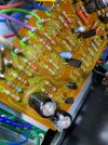


Something is completely screwed up with your work.
I hope you have a spare SC945, so you can test again the pin out.
You have to find standard procedure how you identify transistors on your desk, how to find the correct pin out, install it on the board and recheck the pin out before you start soldering.
For me the only certain way is my standard step by step approach.
If there a different transistor types required, I always work with one type at a time. First get the right numbers, test at last one with the little transistor tester, print facing towards me AND write down the displayed pin out.
Recheck ones more that I have a NPN or PNP, if hFE and Uf is required as well. Only after that is confirmed, I adjust the legs to the board layout, and take my time to match the displayed pin out with the print on the board.
Last thing before I solder all three legs. Start with only one leg, then turn to the part side and try to position the transistor in a most favorable position, that you can easily read the numbers for a later test.
The picture below shows how I prepare the transistors, AND you can see, that the SC945 I have on my desk are ECB pin out with the flat side facing me.
I haven't seen a SC945 with a CEB pin out so far.
Attachments


Last edited: