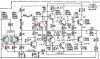
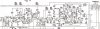
Here we have much fun in perspective!
In the original circuit, the base resistance on TR601 is high, 120k. But on the feedback side, this is much lower at 22k (R609). In order to have low offset voltage, the collector currents in TR601 and TR602 must be different. And different, they are!
With the original value for R605, the collector current in TR601 is very small, at ~0.15mA. The rest of the tail current, which is ~1.9ma flows by TR602. So, the collector current in TR602 is ~1.75mA, or if you prefer ~12 times as large as the collector current in TR601. I neglected the base current in TR603.
The conflictual relationship between low distortion (equal collector current in the differential stage) and low output offset voltage is evident in this particular design.
Reducing R605, as BinaryMike suggested, is a good point for balancing the differential stage, but if the components on the feedback side are not changed you will have an offset high in the sky... You must also change R609 for a 120k, R601 for a 4k5 (to keep the same gain, but you can change it to another value if you want to change the gain), C605 can be lowered to 10uF. This is assuming a matched (hFE) pair for TR601/TR602.
The voltage on the collector of TR602 (-38V) is wrong, it is approximately the same as the emitter voltage of TR603, certainly not more negative.