Hey folks -
I guess I'm easily distracted... I've been working on my own copy of the @kward bench power supply, and in the back of my mind is this EL84M amp based on Heathkit AA-100 iron that I've been nudging along ever so slowly.
I've done a few design iterations of the power supply for the amp in simulation, and I have been planning on doing a regulated supply. But the work on the bench supply made me think -- hey, maybe I should take a crack at a Maida-style power supply using a power MOSFET rather than the 6550 array... From Kevin's earlier bench power supply thread, I know he had trouble with solid state pass device, but it's not like this thing has to stand up to the rigors of a bench unit!
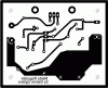
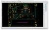
Now, having made the bench supply boards on thru-plated perf boards, I don't care to really care to do that again... especially since if I like it I'll stick with it... and with small runs of custom PCBs being so cheap these days, that's what I'm going to do.
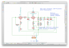
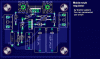
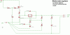
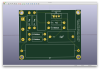
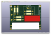
This is basically the floating LM317 section from Kevin's bench supply, but controlling a 700V 8A IXYS power MOSFET rather than the 6550 array in Kevin's unit or the Darlington voltage follower in the original Maida design. Rather than the adjustment pots, there are 4 footprints for resistors for the adjustment divider -- an upper leg of 2 parallel resistors, and a lower leg of 2 parallel resistors. The parallel pairs provide some flexibility in fine-tuning the divider ... or you can use flying leads to an external adjuster network if you really need to. The lower leg of the divider has footprints for vertically-mounted wire-wound power resistors, because they'll have to dissipate some heat... in the case of my EL84M amp, 300 upper and 100K lower for 421V results in the lower leg dissipating a continuous 1.8W.
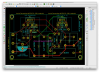
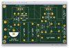
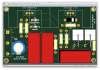
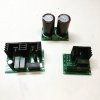
I put the 2 TO-220 packages on individual Aavid Thermalloy heat sinks that are flat on the back, and flush with the edge of the board. The idea is that you can mount the the board standalone or attach the heat sinks to your metal chassis if extra heat sinking is required.
This board doesn't do it all... in particular, you need to have a reservoir cap after the rectifier, and you can also use a small value power resistor (33 Ohms in my case study) to handle some of the workload at higher currents so that the MOSFET doesn't have to dissipate so much power. Those are left as an exercise for the reader, as are the upper and lower divider resistor values for your specific application.
As for capacitors, I'm using a 10,000 hour Nichicon electrolytic for the output reservoir, and Panasonic rectangular polypropylenes in the film cap positions. None of the resistors require anything better than 5% tolerance, except the adjustment divider, but only because you want predictable results. The only exotic components are the 9.1V Zener and the 22V TVS diode -- and they're not especially exotic.
I spec'd a 600V-rated TE AMP 3-position screw terminal block with a 10.16mm pitch, but you could skip that entirely and just solder flying leads if you like. Mouser doesn't sock these, but they're readily available at Digi-Key.
I'm about to submit the Gerbers for the initial test run of these boards, so the "completely untested" grain of salt applies... but I've already had one friend inquire about kits. I could certainly entertain that if there's sufficient interest.
Feedback welcome.
I guess I'm easily distracted... I've been working on my own copy of the @kward bench power supply, and in the back of my mind is this EL84M amp based on Heathkit AA-100 iron that I've been nudging along ever so slowly.
I've done a few design iterations of the power supply for the amp in simulation, and I have been planning on doing a regulated supply. But the work on the bench supply made me think -- hey, maybe I should take a crack at a Maida-style power supply using a power MOSFET rather than the 6550 array... From Kevin's earlier bench power supply thread, I know he had trouble with solid state pass device, but it's not like this thing has to stand up to the rigors of a bench unit!
Now, having made the bench supply boards on thru-plated perf boards, I don't care to really care to do that again... especially since if I like it I'll stick with it... and with small runs of custom PCBs being so cheap these days, that's what I'm going to do.
This is basically the floating LM317 section from Kevin's bench supply, but controlling a 700V 8A IXYS power MOSFET rather than the 6550 array in Kevin's unit or the Darlington voltage follower in the original Maida design. Rather than the adjustment pots, there are 4 footprints for resistors for the adjustment divider -- an upper leg of 2 parallel resistors, and a lower leg of 2 parallel resistors. The parallel pairs provide some flexibility in fine-tuning the divider ... or you can use flying leads to an external adjuster network if you really need to. The lower leg of the divider has footprints for vertically-mounted wire-wound power resistors, because they'll have to dissipate some heat... in the case of my EL84M amp, 300 upper and 100K lower for 421V results in the lower leg dissipating a continuous 1.8W.
I put the 2 TO-220 packages on individual Aavid Thermalloy heat sinks that are flat on the back, and flush with the edge of the board. The idea is that you can mount the the board standalone or attach the heat sinks to your metal chassis if extra heat sinking is required.
This board doesn't do it all... in particular, you need to have a reservoir cap after the rectifier, and you can also use a small value power resistor (33 Ohms in my case study) to handle some of the workload at higher currents so that the MOSFET doesn't have to dissipate so much power. Those are left as an exercise for the reader, as are the upper and lower divider resistor values for your specific application.
As for capacitors, I'm using a 10,000 hour Nichicon electrolytic for the output reservoir, and Panasonic rectangular polypropylenes in the film cap positions. None of the resistors require anything better than 5% tolerance, except the adjustment divider, but only because you want predictable results. The only exotic components are the 9.1V Zener and the 22V TVS diode -- and they're not especially exotic.
I spec'd a 600V-rated TE AMP 3-position screw terminal block with a 10.16mm pitch, but you could skip that entirely and just solder flying leads if you like. Mouser doesn't sock these, but they're readily available at Digi-Key.
I'm about to submit the Gerbers for the initial test run of these boards, so the "completely untested" grain of salt applies... but I've already had one friend inquire about kits. I could certainly entertain that if there's sufficient interest.
Feedback welcome.