• The move to the new server is done. There are some software and database maintenance updates in process. This has us passing the hat around to help out. We appreciate any donations. Seriously, even a dollar helps. The payment page may be found here - https://www.audiokarma.org/support.html

SA-710 - total rebuild, blowing protection transistors

QSilver

Super Member
Picked up an SA-710 which powered up okay but on testing, I found all outputs and driver transistors blown open and the transistors to detect over-current, DC and engaging the relay to be blown open too. The over-current ones were literally cracked in half!

I've rebuilt it using new output transistors and driver transistors. I used KSA1220/KSC2690 as the drivers - this amp has a similar topology as the x800 series amps but without the NSA section so I thought it might be worth trying these in. Using MJL1381 and counterpart as outputs. Everything seems to look good. Low DC offset, idle current isn't going out of control... Distortion measures under 0.02%....

But when powering without DBT, the protection relay clicks in then out immediately and I find that Q31 and Q32 are blown open, holding the amp in protection while the amp sits stable.

At a loss as to why this is happening. Anyone have any ideas?
 

Attachments

Register to hide this ad
The enclosed schematic is unreadable.

I have a copy of the sa-710s.pdf and there is no Q31 or Q32 as far as I can tell. Q30 is the highest it goes.
 
I've uploaded a PDF copy - took me a few attempts to compress it enough to upload. hopefully that's legible now. This is the schematic from the SA-710 supplement service manual for the UK version. It has the addition of Q31 and Q32 next to the output transistors on the schematic.

EDIT: Transistor Info.

As I said most transistors in the amp were dead so I had to replace a lot. Below is a list of subs I used. Maybe this is where I'm going wrong. I originally said I was using MJL output but seems I have actually used Toshiba outputs instead - I fitted them a while back now and left this on a shelf.

Outputs - Q1 - 2SC2525 - 2SC5242
Q3 - 2SA1075 - 2SA1962
Drivers - Q21 - 2SC2275 - KSC2690 OR 2SC5171
Q23 - 2SA985 - KSA1220 OR 2SA1930
Pre-Driver/ Q17 2SA912 - KSA1013
VAS? Q19 2SC1885 - KSC2383

Q15 - 2SC1775A - KSC1845

Q31 and Q32 are both KSC1845, I replaced the blown emitter resistors with new 0.47R resistors.

The STV3H tests good but with it in the idle current went into thermal runaway so currently that's been replaced with a KSC3503 with the collector and base connected together to act as a diode. I replaced the "cut jumper wire" for the bias with a 100 ohm trimpot and i can adjust the bias which does not run away anymore but is VERY sensitive to current limiting.
 
Last edited:
ok, I see Q31 & Q32, used as overload detectors off if the emitter resistors of the outputs.

You did not replace them when you did all the other transistors? Also, what about C88 & C89?

When the emitter resistors popped, Q31 / Q32 could have been subject to 48 volts through the 4.7k / 15k /diode dividers.
Transistors that get more than a max of 5 volts emitter to base are destroyed.
They LIKE 0.6v and after being turned on by the 0.6v, very SMALL increases in base current control the collector to emitter current. Thus to say small currents are also small voltages. Over 5 volts is destructive overkill.

Replace them, test all those resistors AND diodes around them, and check that the caps aren't Sanyo;s - film caps would be best.

TL/DR: popped emitter resistors allowed them to blowup, and they weren't replaced.
 
The caps were replaced before powering up for the first time - they're film types. The original transistors were cracked in half in the Q31 and Q32 positions so they've been KSC1845's since first power up - as well as new emitter resistors - there wasn't much left of the amp that wasn't blown so all the transistors in the power amp, pre-amp, phono amp and protection were replaced. together with all caps except the big filter caps for now.

I'll double check the resistors around the transistors (4.7k and 15k) and the diodes.

I'm not 100% sure I've got the bias stage working correctly with my setup. I can bias the amplifier but I get very low distortion - less than 0.05% even down to less than 1mV of bias. Maybe thats fine? Just not what I was expecting.

Side note: The first time it happened I replaced the KSC1845's and tested the amp - back on DBT - driving it to 10W and checking distortion. To do this the DBT was allowing around 150W. One channel was at 0.04% - the one with KSA1220/KSC2690 so I checked the switches to see if the would make a difference. I flicked the loudness switch back and forth a few times and then the protection went and the overload detector transistor for that channel only was blown again. Maybe this is helpful backstory.
 
Both 4.7k and 15k resistors around both Q31 and Q32 test good at 4.6k and 14.9k respectively. I've also tested the didoes, in circuit with a diode test and these seem to test good. But I could replace anyway? I need to order some more 1N4148's... While testing, the transistors have been removed - they were blown anyway.
 
I've got more 1N4148's. Should I go ahead and replace the diodes and put two new KSC1845's in Q31 and Q32 or is there more testing worth doing? I'm wondering if looking for a voltage pulse on power up with a scope might be worth doing...?
 
replacing diodes won't hurt... in fact I recommend it.

BUT REMEMBER, that's NOT a ground at the emitters, it's the amplifier outputs.

now, is it the base, or the collector getting too much juice?

What I would do is to power it up the first time with the Q31 & Q32 positions empty.
I would hook up a DMM to watch the base to emitter voltage. Then repeat looking at the collector to emitter voltage.

I might even go as far as make a diode analog of an npn transistor and put that in there.
Two diodes, anodes connected and that's also the base connection, the cathodes are emitter and collectors.
Who knows, it might smoke the base to emitter diode. See if the other diode survives.

The resistances in the circuit say "no", 15k and 4.7k to the base, collector has a 68k pullup on the other side of D7.The emitters are the amp outputs.
But Q31 & Q32 WERE cracked in half. That takes some juice.
 
Testing the transistors that I've removed from the Q31 and Q32 positions, I have three (lost the fourth one) they've all failed in the same way. Putting them on a diode test,

C-B junction: Positive Base, Negative Collector: 0.6. Inverted: 0.8
C-E Junction: Open circuit in both directions.
E-B Junction: Open circuit in both directions.

I used a digital scope to measure the voltage at power on. Referenced to ground.
With the diodes connected where Q31 and Q32 as you suggested, I get a large peak on the collector. For around 300ms theres a big spike over 25.6V (scope clipped at that voltage) then the voltage drops to 0 before steadily rising back up to 15V over around 3 seconds.

The Base, at around the same time has a clipped peak of 25.5V for around 300ms again, then drops sharply to -6.5V then rises back to 0 with a slight peak over to a low positive voltage over another 300ms.

Perhaps this -6.5V is what might be damaging the Base?
 
what is the amp output doing at that time? Remember these are differential signals referenced to the amplifier output, not ground.

Q31 & Q32 emitters are tied to the respective amplifier output.

You say "total rebuild", transistors, diodes and caps in all the power supply sections? meaning that the PS is sequencing properly.
 
At the time of those voltages, the amp is powering up. During these tests, I ran the amp without DBT and discharged the main capacitors between power cycles as these are the conditions that the transistors are most often blown.

Total rebuild. I will double check, but all the transistors within the power amp with the exception of the differential input transistors, the small "pre-amp" section comprising of three transistors per channel, and the phono stage also got new transistors. The protection circuit is all new transistors. I've been through it and replaced all the small signal diodes in the protection circuit today. All the capacitors besides the two large filter caps have been replaced with new Nichicon PW or Panasonic FC. I've used film for smaller values and Nichicon KL where low esr caps were situated. The emitter resistors have been replaced too.

I don't think I have replaced any transistors within the power supply as of yet and no zener diodes.

I still have all the dead components in a jar somewhere so I can back track if needs be.

Remember these are differential signals referenced to the amplifier output, not ground

Perhaps I should retake these measurements with that in mind? I had a feeling that may be the case but elected to use the scope as it can react much faster than my DMM. Perhaps I could use one channel to measure the amp output and another to measure the collector or base and then use a math function to give the resulting voltage?
 
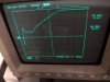
I've retaken those measurements with the Math function. One probe on Collector or Base and the other on the output before the inductor. Then displayed the result from Collector/Base subtract Output. I got the following graphs on amplifier power up from cold (drained main capacitors)

Just to check, I then powered the amplifier off and on again without draining the caps and the two negative spikes on the Base graph were not present.
 

Attachments

  • Base-vs-Output.jpg
    Base-vs-Output.jpg
    62.3 KB · Views: 12
  • Collector-vs-Output.jpg
    Collector-vs-Output.jpg
    74.2 KB · Views: 11
just two channels, right?

Do the same thing,but to the unregulated +/- 49v then the +/- 32v regulated supplies

then do a ground based reading for each output channel.

All during a cold turn-on.
 
Two channel scope? Yes.

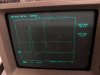
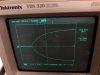
Both unregulated power supplies measured from the main capacitors with a x10 probe. Both look ok...

Measured both regulated supplies - both start operating at the same time, the voltage on the positive regulator is a little low - 30V vs 33V but thats the only difference I can find.

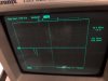
Probing the outputs before the inductor on both channels shows nearly identical results. With the left channel trace looking slightly noisier than the right channel. Both channels hit a peak of 48.2V and 48V respectively and then drop to a negative peak of -5.8V and -5.2V respectively. I used the Ref to save the channel output graphs and lower the 0V point so as to see the top of the waveform of each.
 

Attachments

  • Left-Channel.jpg
    Left-Channel.jpg
    67.5 KB · Views: 9
  • Regulated-PSUs.jpg
    Regulated-PSUs.jpg
    72.1 KB · Views: 8
  • Right-Channel.jpg
    Right-Channel.jpg
    69.9 KB · Views: 9
  • Unregulated-PSUs.jpg
    Unregulated-PSUs.jpg
    77.7 KB · Views: 8
Back
Top Bottom