• The move to the new server is done. There are some software and database maintenance updates in process. This has us passing the hat around to help out. We appreciate any donations. Seriously, even a dollar helps. The payment page may be found here - https://www.audiokarma.org/support.html

SA-8800 with Bias Splitter problem

GlasgowGrip

Sound just like a record on the phonograph
Subscriber
Hello all,

I've bought myself a problem child SA-8800 from the 'bay, with a sickly Right channel in the Power Amp section. I'm at the point in my troubleshooting where I need to ask for help. I've been scouring SA-8800/SA-9800/SX-3900 threads and have learned quite a lot about NSA amps and made some good progress, but... I'm frustrated and considering just shotgunning all the rest of the Right channel silicon on the P.A. board instead of working the problem, but I'd much prefer to ask for help understanding the final pieces of the NSA puzzle. So if @markthefixer or any other NSA expert might be so kind as to assist with the remaining detective work, I'd be eternally grateful!

The good news is that I've done a lot of the legwork and have the rest of the amp pretty well sorted.

The good news (so far):
  • Repaired and recapped Power Supply board (AWR-182): found cracked solder joints at several transistors; replaced relay/protection circuit transistors Q1-Q4; Voltages are now solid.
  • Upgraded power lamp to LED with SMD bridge rectifier (included swapping out R18-R19 for a single 11kOhm 1/2W metal film; LED drawing 3.9mA, new R is dissipating 165mW)
  • Recapped TC Assembly (GWG-122)
  • Recapped EQ Assembly (GWF-113)
  • Recapped Indicator Assembly (AWV-001)
  • At this point, the Preamp is working great and measures well: THD+N L=0.0045%, R=0.0049%; Freq Response flat within 0.5dB from 20-20kHz
  • Recapped Power Amp (GWH-115) and replaced all trimmers VR5-VR10 with Bourns cermets.
  • P.A. Left channel: Still all-original Drivers and Outputs on Left channel - cleaned the micas and regreased the Left Outputs when I had the heatsink out for cleaning. Left Channel offset dials in fine and Bias sets as per service manual - Left Channel is working and solid!

The bad news:
  • P.A. Right channel had issues when I bought the unit. DC Offset (250mV) and Bias (950mV) were running way too high. The Drivers were not original, and someone had clearly tried to reflow all the transistor and diode solder joints on the Right channel. One of the trimmers had been removed and reinstalled in the wrong orientation. Even after getting the offset adjusted and reorienting that trimmer, the bias would still not come down and conclusion was output(s) likely compromised. And since someone had already tried subbing in newer Drivers, I just pulled all the Right channel Outputs and Drivers.

Present status of Right channel Power Amp:
  • My ultimate plan is to replace the Right channel Outputs with onsemi NJW0281G/NJW0302G, but I won't be installing them until I can get the Bias/Driver voltages corrected.
  • replacements made so far on Right Channel...
    • Q40/Q42 (Drivers) - TTC004B/TTA004B
    • Q14 (emitter follower buffer) - KSA992FTA
    • Q16 (VAS/Predriver) - KSC3503DSTU
    • Q18 (7ma Current source) - KSA1381ESTU
    • D12/D14 ("failsafe" diodes) - 1N4004
  • have removed all Power Limiter transistors Q32/Q36/Q34/Q38 - all test good - am leaving out of circuit until Bias mystery is solved.
  • have been testing everything else on the board - resistors, diodes, other transistors - everything seems to measure good
  • the Differential input section Q8/Q10/Q12 seems to check out okay
  • the VAS section Q14/Q16 checks out (Q14/16 replaced see above)
  • the 7mA current source Q18 checks out (Q18 replaced see above)
  • the Current sources Q28/Q30 seem to check out okay
  • this seems to leave me with the Bias Splitter / NSA circuits. This is where things are still fuzzy in my comprehension.

Okay, time for Right channel troubleshooting measurements... Test conditions are on full line voltage (no DBT), with VR8 and VR10 full-CCW (at min resistance), no Outputs and no power limiters (Q32-Q38). These measurements are given based on another MTF thread, since my best assessment is this appears to be a Bias Splitter or NSA circuit problem with excess voltage coming in from somewhere. I'm more than happy to provide measurements of anything else, pictures, etc, - just trying to jumpstart the discussion:

with VR8 Full CCW (min R)...
anode/cathode/Vd​
D8: -3.318 2.249 -5.567​
D10 (STV-2H): 0.354 -0.750 1.104​

V1/V2/Vr​
R84: 2.249 3.875 1.626​
R86: -3.328 -4.988 -1.660​
B/C/E​
Q40 Driver NPN: 2.084 48.06 1.522​
Q42 Driver PNP: -3.168 -48.38 -2.608​
Q40/42 B-to-B: 5.252​
Q40/42 E-to-E: 4.130​

with VR8 Full CW (max R)...
anode/cathode/Vd​
D8: -3.351 2.473 -5.824​
D10 (STV-2H): 0.675 -0.420 1.095​
V1/V2/Vr​
R84: 2.474 4.101 1.627​
R86: -3.355 -5.017 -1.662​
B/C/E​
Q40 Driver NPN: 2.308 48.15 1.748​
Q42 Driver PNP: -3.189 -48.51 -2.631​
Q40/42 B-to-B: 5.497​
Q40/42 E-to-E: 4.379​
Thanks in advance, cheers! - Steve
 
Register to hide this ad
Quick update, I went ahead and pulled the four NSA transistors, Q20/24 and Q22/26, and they all measure good on a Peak Atlas DCA75. The connected resistors all measure within 2% or better of nominal. Going to go ahead and just replace with KSA992/KSC1845 since I have them pulled and will report back.
 
Have you seen the A-9 thread?b It's 29 pages long, with some good attachments by me.

RE: current sources Q28 & Q30. they exist solely to supply a voltage to the bases of Q24 & Q26, slightly above and below (diode drop + 100Ω / 1mA current) the "output voltage". The current (VR10) controls the magnitude of the voltage. which is the second bias set point.
 
Last edited:
Have you seen the A-9 thread?b It's 29 pages long, with some good attachments by me.

RE: current sources Q28 & Q30. they exist solely to supply a voltage to the bases of Q24 & Q26, slightly above and below (diode drop + 100Ω / 1mA current) the "output voltage". The current (VR10) controls the magnitude of the voltage.
Hi Mark - thanks for checking in. Not sure about that A-9 thread - I'm gonna say no, but I will seek it out shortly.

In the meantime, quick update - replaced Q22, Q24 with KSA992FTA and replaced Q20, Q26 with KSC1845FTA and only marginal improvement.
Q40/42 B-to-B: 5.275​
Q40/42 E-to-E: 4.176​

But here's something: I did also just a quick check on Q28 and Q30 - things seem wonky there! I missed the boat earlier on comparing their emitters to the regulated rail voltages. Doh! Here we go...
Q28 Emitter to Pin 25 = 2.033V​
Q30 Emitter to Pin 26 = 2.056V​
(not sure which relative polarity you're looking for, but magnitudes are obviously off - is the nominal 0.7?)

For comparison, just checked the counterparts on the Left channel:
Q27 Emitter to Pin 25 = 1.220V​
Q29 Emitter to Pin 26 = 1.217V​
 
Last edited:
check VR9 & VR10 for correct CCW resistance.

Q28 & Q30 = VR10
Q27 & Q29= VR9
 
VR10 is full CCW, confirmed it measures 0.4 ohms

And sorry I hurriedly threw in the Left channel comparison, I should've made clear that the Left channel is operational and is currently adjusted for correct Bias (70mv).
VR9 is currently adjusted for 70mV bias on left channel and is measuring 32.81 kohms
 
Sure thing, these measurements taken relative to the "outputs", Left channel (D9) black lead on Pin 15, Right channel (D10) black lead on Pin 20

anode/cathode/Vd
L - D9 (STV-2H): 0.599 -0.555 1.154
R - D10 (STV-2H): 0.363 -0.778 1.141

L trimmers (VR7/VR9) are adjusted per SM for nominal bias reading (70mv).
R trimmers (VR8/VR10) are full CCW, minimum R.
 
let's concentrate on the Right Channel (duff) Q28 & Q30 circuits, compared to the Q27 & Q29 circuit readings.
when examining the current sources, the reference voltage should be the "nearby" rail for that polarity.
when examining the diode / resistor string, the reference should be the output terminal (common point of all emitter resistors)

oodles of voltage measurements, focusing on the base string dominated by the 47k resistor.
that establishes the currents through the resistors and diodes to set the base voltages of the current sources.
emitter too high means base too high with the 1k and diodes seeing more current than they should.

You have checked all transistors for function, and resistors for value (hopefully BOTH out of circuit).

The chances of a pc board fault are climbing, ASSUMING that when reinstalled the transistors and resistors are resoldered well.

For that, I run ohmmeter tests from component lead to component lead. A bad foil or solder joint then sticks out.

keep the power limiters out of circuit for now.
 
Last edited:
@markthefixer: Understood Mark, I will attack this in the morning and post detailed measurements of the Q28/30 and Q27/29 current sources and their diode/resistor strings.

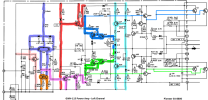
By the way, I have been studying more of your posts on NSA topology and troubleshooting, in particular this one about the keys to the SX-3900 kingdom. I've taken the liberty of following your lead and created a colorized schematic for the Left channel of the SA-8800, mainly for my own edification but maybe it will be useful here or for someone else in the future. Please advise if I got anything wrong - thanks!
Pio_SA-8800_PowerAmpLeftChannelSchema-Colorized.png
 
looks ok, waiting on the R109 47k Ω (yellow violet orange gold) divider voltages.

But here's something: I did also just a quick check on Q28 and Q30 - things seem wonky there! I missed the boat earlier on comparing their emitters to the regulated rail voltages. Doh! Here we go...
Q28 Emitter to Pin 25 = 2.033V
Q30 Emitter to Pin 26 = 2.056V
(not sure which relative polarity you're looking for, but magnitudes are obviously off - is the nominal 0.7?)

For comparison, just checked the counterparts on the Left channel:
Q27 Emitter to Pin 25 = 1.220V
Q29 Emitter to Pin 26 = 1.217v
When checking the right (duff) channel read for BOTH extremes of the VR10 68k Ω trimpot.
 
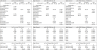
Bit of a struggle with how to best present all these measurements, tried posting an image but it gets downsized too much...

So just attaching a pdf. Hopefully this will suit you, if not, please just let me know and I'll paste in long lists of measurements. Thanks!
 

Attachments

I thought by now you would see it.

VR10 is NOT acting the same as VR9. or how you operated VR9

They seem to be in opposition to each other.

your CCW on VR10 is scorchingly high bias R100 2.029v
while CW on VR10 reduces the bias. R100 0.671v


It is a bit counter-intuitive. more resistance lowers current in the biasing string, cutting the voltage across R108 & R112
this reduced voltage translates into reduced voltage / current from the current sources.
 
Last edited:
Yes, I see the numbers but they didn't make sense - I feel like I'm still trying to fully grok the current source/resistor/diode chains and how it all interacts with the NSA transistor pairs. I mean, I think I understand, right up until when I try to figure out where the extra voltage could be coming from.

I will triple-check the VR10 trimmer orientation shortly, as soon as I get back to the bench. But even if wrong, I still don't think that would explain the high Base and Emitter voltages on the Drivers Q40/Q42 (and the high Base-to-Base and Emitter-to-Emitter voltages across the Drivers), does it? If it was as simple as backwards trimmer action, wouldn't they come down to normal or below when full CW?

Background: I'm referring to the currently ongoing SA-9800 Help thread and the cool diagram you posted there. The Driver voltages on my working Left channel (Q39/Q41) do match up to that diagram.

Thanks a million for your patience, Mark! Will report back with details on trimmers VR7-VR10.
 
Those transistor current sources set operating points for the NSA bias splitter circuits, which then develop the base drive voltages for the output transistor's drivers.
 
@markthefixer: Yessir, I think I'm sound on the basics of the topology and theory of operation (mostly thanks to several of your detailed explanations in previous threads). But trying to troubleshoot it is not making sense. I've re-re-confirmed that the trimpots are installed as per the schematic, and I've confirmed the resistance measurements that seem to me to be correct. VR9 and VR10 are both measuring as a short (0.4 ohms) across the traces when full CCW (counterclockwise). VR9 measures 101k ohms and VR10 measures 103k ohms across the traces when fully CW (clockwise). Photo to show the actual orientations...
2023-09-08_19.01.47.jpg

Also, more updates: I have been going through the circuit board with a magnifier and also probing for voltages and continuity as you described, and so far have not been able to identify any broken, cracked or damaged traces, joints or component leads.

I also went ahead and did some more shotgunning:
  • Replaced Q28 with KSA992FTA and replaced Q30 with KSC1845FTA.
  • Replaced R110 with 47kΩ 0.5W 1% Metal Film (Vishay Dale CMF5547K000FHEK).
  • Replaced D20 and D22 with onsemi 1N4448.
All the above components I removed did test successfully, but I replaced them anyway.

Still no joy, essentially no improvement at the Drivers

Right Driversref. to R Output (blk to Pin 20)Right Driversref. to R Output (blk to Pin 20)
VR10 CCW (min. R)BCEVR10 CW (max. R=103k)BCE
Q40 Driver NPN2.05648.431.507Q40 Driver NPN2.10249.021.551
Q42 Driver PNP-3.223-48.91-2.68Q42 Driver PNP-3.193-49.37-2.647
B-to-B:5.279E-to-E:4.187B-to-B:5.295E-to-E:4.198
 
What are the ACTUAL Bournes parts numbers of VR5, VR6, VR7, VR8, VR9 & VR10.
 
It is getting to be time to swap the outputs (and ONLY the outputs) channel to channel.

If you have a transistor tester that reports Hfe and Vbe , get them for all 8.

Take the unruly pairs (4 of them) and bring them up on the well behaved channel.

Then take the well behaved pairs (4 of them) and bring them up on the unruly channel.

DO NOT USE THE CCW DIRECTIONS ON THE UNRULY CHANNEL, USE A dmm TO GET THE CURRENT SOURCE VBE'S TO MATCH THE WELL BEHAVED CHANNEL.
 
Last edited:
This has all been done with no outputs on the bad channel. I have modern TO-3P replacements (NJW0281G, NJW0302G) ready to go in, but wanted to figure out the bias issues first.

Trimmers:
VR5, VR6 DC Offset 2 Resistor Trimmer 330kΩ 0.5W 3386F-1-254LF Bourns 250kΩ 0.5W 10% Cermet Trimmer 3/8" Top Adjust
VR7, VR8 Bias 56mV 2 Resistor Trimmer 100Ω 0.5W 3296Y-1-101LF Bourns 100Ω 0.5W 10% Cermet Trimmer 25-turn Top Adjust
VR9, VR10 Bias 70mV 2 Resistor Trimmer 68kΩ 0.5W 3296Y-1-104LF Bourns 100kΩ 0.5W 10% Cermet Trimmer 25-turn Top Adjust

I know the offset pots are lower than original but so far it looks like I don't need anything near 330k to balance. And yes the offset pots have reversed rotation from the originals.
 
try them without enough base current (vr10 to fully cw) to light them up.

there are a pair of resistors before the base drives - their drop is important.

no where near enough resources to get technical now.

post #13 is EMPHASIZED.....

vr10 is acting backwards, with minimum base drive at fully cw.
 
Back
Top Bottom