Fabio92
New Member
Hi all, this is my first help request in this forum and I hope in somewone kind advice. About two weeks ago my friend gave me a SA-9800 saying that the left channel sounds distorted. I'm not familiar with this particular model but i wanted to give it a try to fix.
Before powering the unit I readed the service manual, to have a general idea of what might be the problem. After reading several posts here on AK about the PSU heating problem and component failure I started form there checking all the voltages.
The amply was untouched, all original. Moreover it seems it was not used so much, the PSU pcb is in a good state, no burnings, no brown areas. I already now that a complete recap is quite mandatory, even if not stressed, electrolitic capacitors have almost 42 years and leakage current and ESR might be a problem.
PSU assembly is the awr-196 and voltages at the outputs are quite good, mabe +18V to display a litte out specs:
pins 1&2 -52V -52.71V
pins 3&4 +52V +52.46V
pins 5&6 +32V +32.72V
pin 7 +18V +19.34V
pins 10&11 -32V -32.72V
input voltages
pin 17 55.4Vrms
pin 18 55.5Vrms
+68V is actually 73.7V
-68V is -75.6V
Outputs from the rectifier board awr-191 are a little out:
pin 13 -55V -59.9V
pin 14 55V 58.88V
pin 16 55V 59.7V
pin 17 -55V -59.9V
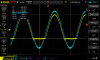
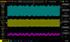
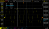
Then I moved to the pa-L assembly gwh-119. The first check I've made was hooking an oscilloscope probe to the outputs in parallel with a small speaker. Given a sine 1kHz input, just starting from very low volume adjustment, the left output is clipping to about -740mV. Attached a comparison betwheen left (yellow) and right (cyan) outputs.
It's not possible to regulate idle current, I always measure 8.8mV at pins 37-39 and 0v beetween 38-40. Dc offset is instead adjustable and at 5.3mV.
Note: all the measurement noted before desoldering components and reported on the image below are still the same even after re-soldering original components.
I started looking for damaged componets or cold joints on the pa-L assembly. I've disconnected the four output bjt (2SA1076 & 2SC2526) and tested BE and BC junctions with a multimeter giving about the same readings of Veb = 0.558V, Vcb = 0.548 for the pnp and Vbe = 0.579, Vce = 0.577 of the npn. Then I moved to the drivers 2SA913 & 2SAC1913 and they still seems good. Of course I've cheched that there weren't CE shorts. I've desoldered and checked in the same manner almost every transistor, except the monolithic current mirror and input differential pair. I've also checked every resistor with "one leg out" rule and they are on specs. Honestly I'm starting loosing ideas! The output wave is still clipping at about -730mV. I also disconneted pin 26 form the protection assempby witout any changes.
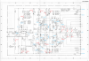
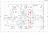
I measured most of the interesting currents/voltages in the circuit as reported in the image attached and below (currents are derived from voltages and previous resistance measurements):
emitter current of the differential pair: 570uA (500uA)
emitter currents of Q5 mirror, equally spread on both bjt is 283uA
Ir23 & Ir29 (top left current source) respectively 983uA (1mA) and 7.25mA (7mA)
Ir47 & Ir55 (top current source) respectively 1mA (1mA) and 1mA (1mA)
Ir35 & Ir59 (bottom current source) respectively 1mA (1mA) and 1mA
pin 26 (no load) 0v
Current throught balancing emitter resistor R79,83,81,85 0A.
D5 cathod 1.23V (1.5V)
Q7's collector 4.38V (4.5V)
Q33's base 1.17V (1.17V)
Q25,Q27 protection bjt both off
here I'm starting having throubles:
D5 anode -4.77V (-1.5V)
Q11's collector -15.37V (-4.5V)
Q11'emitter -47.5V (-50.5V)
Q33's base -0.91V (-1.4)
Q29,Q31 protection bjt both fully on
current throught Q11's collector resistance R33 24.6mA
Q13 Vbe 635mV
Q15 Vbe -490mV
Q17 Vbe -358mV (too low conducting)
Q19 Vbe 630mV (too conducting)
The negative side of the circuit is pulling too much current. I think It's not the driver Q35 because is barely conducting with a Vbe of -540mV.
My guess is that the culprits are the protection bjt Q31 & Q29 but I can't figure way they are conductiong.. Q29 Vbe is given by the the Wheatstone bridge at the output but load current is 0A.
Finally I did somethig that phreaps someone can judje crazy, but I turned the power on without Q29 & Q31 but in this case the situation was revesed putting into conduction upper Q27 & Q25 protection transistor turning off Q33 driver.
I very appreciate if someone followed me till the end, I spend several hours trying to figure out what is going and I wanted to give most details as possible hoping for your kind advice.
Before powering the unit I readed the service manual, to have a general idea of what might be the problem. After reading several posts here on AK about the PSU heating problem and component failure I started form there checking all the voltages.
The amply was untouched, all original. Moreover it seems it was not used so much, the PSU pcb is in a good state, no burnings, no brown areas. I already now that a complete recap is quite mandatory, even if not stressed, electrolitic capacitors have almost 42 years and leakage current and ESR might be a problem.
PSU assembly is the awr-196 and voltages at the outputs are quite good, mabe +18V to display a litte out specs:
pins 1&2 -52V -52.71V
pins 3&4 +52V +52.46V
pins 5&6 +32V +32.72V
pin 7 +18V +19.34V
pins 10&11 -32V -32.72V
input voltages
pin 17 55.4Vrms
pin 18 55.5Vrms
+68V is actually 73.7V
-68V is -75.6V
Outputs from the rectifier board awr-191 are a little out:
pin 13 -55V -59.9V
pin 14 55V 58.88V
pin 16 55V 59.7V
pin 17 -55V -59.9V
Then I moved to the pa-L assembly gwh-119. The first check I've made was hooking an oscilloscope probe to the outputs in parallel with a small speaker. Given a sine 1kHz input, just starting from very low volume adjustment, the left output is clipping to about -740mV. Attached a comparison betwheen left (yellow) and right (cyan) outputs.
It's not possible to regulate idle current, I always measure 8.8mV at pins 37-39 and 0v beetween 38-40. Dc offset is instead adjustable and at 5.3mV.
Note: all the measurement noted before desoldering components and reported on the image below are still the same even after re-soldering original components.
I started looking for damaged componets or cold joints on the pa-L assembly. I've disconnected the four output bjt (2SA1076 & 2SC2526) and tested BE and BC junctions with a multimeter giving about the same readings of Veb = 0.558V, Vcb = 0.548 for the pnp and Vbe = 0.579, Vce = 0.577 of the npn. Then I moved to the drivers 2SA913 & 2SAC1913 and they still seems good. Of course I've cheched that there weren't CE shorts. I've desoldered and checked in the same manner almost every transistor, except the monolithic current mirror and input differential pair. I've also checked every resistor with "one leg out" rule and they are on specs. Honestly I'm starting loosing ideas! The output wave is still clipping at about -730mV. I also disconneted pin 26 form the protection assempby witout any changes.
I measured most of the interesting currents/voltages in the circuit as reported in the image attached and below (currents are derived from voltages and previous resistance measurements):
emitter current of the differential pair: 570uA (500uA)
emitter currents of Q5 mirror, equally spread on both bjt is 283uA
Ir23 & Ir29 (top left current source) respectively 983uA (1mA) and 7.25mA (7mA)
Ir47 & Ir55 (top current source) respectively 1mA (1mA) and 1mA (1mA)
Ir35 & Ir59 (bottom current source) respectively 1mA (1mA) and 1mA
pin 26 (no load) 0v
Current throught balancing emitter resistor R79,83,81,85 0A.
D5 cathod 1.23V (1.5V)
Q7's collector 4.38V (4.5V)
Q33's base 1.17V (1.17V)
Q25,Q27 protection bjt both off
here I'm starting having throubles:
D5 anode -4.77V (-1.5V)
Q11's collector -15.37V (-4.5V)
Q11'emitter -47.5V (-50.5V)
Q33's base -0.91V (-1.4)
Q29,Q31 protection bjt both fully on
current throught Q11's collector resistance R33 24.6mA
Q13 Vbe 635mV
Q15 Vbe -490mV
Q17 Vbe -358mV (too low conducting)
Q19 Vbe 630mV (too conducting)
The negative side of the circuit is pulling too much current. I think It's not the driver Q35 because is barely conducting with a Vbe of -540mV.
My guess is that the culprits are the protection bjt Q31 & Q29 but I can't figure way they are conductiong.. Q29 Vbe is given by the the Wheatstone bridge at the output but load current is 0A.
Finally I did somethig that phreaps someone can judje crazy, but I turned the power on without Q29 & Q31 but in this case the situation was revesed putting into conduction upper Q27 & Q25 protection transistor turning off Q33 driver.
I very appreciate if someone followed me till the end, I spend several hours trying to figure out what is going and I wanted to give most details as possible hoping for your kind advice.