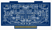
I'm drawing up a PCB to replace an F-2436 board in a 9090 I salvaged from the dump. It works fine as a pre-amp so there's hope for it , but there's no driver board so I need to make one . I have a couple of queries , the first being a request for a sketch or dimensions of the board , so I can get the shape and placement of the two tags that sit up from the top , and also if possible , the shape and dimensions of the bracket the tags fit into since that is missing too. Any help much appreciated.
The second query is : why do many of the boards I've seen photos of , pre and post - restoration , only have one large resistor visible on one channel , the R51 / R52 10ohm 3W ones , I presume the other is behind the board but why ? There is the same amount of room on each side of the PCB it seems to me , I'm puzzled.
The second query is : why do many of the boards I've seen photos of , pre and post - restoration , only have one large resistor visible on one channel , the R51 / R52 10ohm 3W ones , I presume the other is behind the board but why ? There is the same amount of room on each side of the PCB it seems to me , I'm puzzled.