
• The move to the new server is done. There are some software and database maintenance updates in process. This has us passing the hat around to help out. We appreciate any donations. Seriously, even a dollar helps. The payment page may be found here - https://www.audiokarma.org/support.html

Sansui BA-3000 runs super hot when bias set correctly

Tina Louise

Active Member
After a full restoration on my Sansui BA-3000, the left and right F-2507 Driver Circuit boards run super hot when the bias is set correctly at 20mV and on a null load cranked all the way up it will quickly burn up R34 (47ohm) on one of the boards (R33, R35, R36 would shortly follow I'm sure). TR10 (originaly 2SC1669 replaced by KSC2073) and TR11 (2SA839 replaced by KSA940) which are the ones mounted on the heatsink are the components (besides the resistors) that will get very hot.

I bought the BA-3000 in a non-working state so I don't know what the behavior would have been before my changes.

The bias pot on both channels are cranked pretty much all the way clockwise to reach 20mV, by the way. DC offset is as close to 0mV as I can get it.

If I keep the bias pots mostly all the way anti-clockwise (won't even measure any mV), then everything seems happy and the amp runs cool even on a null load cranked all the way up.

I'm getting -64V/+64V (vs -68V/+68V) coming from F-2511 (Protection board) and -69V/+69V (vs -65V/+65V) coming from F-2508 (Power Supply board.

I've replaced all transistors with the substitutes that other people have used on their BA-3000 restoration for driver boards, power supply board, and protection board. The main TO-3 transistors are replaced by the ever popular MJ21195G and MJ21196G (which stay completely cool). All of the zener diodes have been replaced and some of the VD1212 (with dual 1N4148).

F-2507 Driver Circuit

TR01 2SC1400->KSC1845
TR02 2SC1400->KSC1845
TR03 2SA847->KSA992
TR04 2SA818->TTA004B
TR05 2SC1628->TTC004B
TR06 2SC945->KSC1815Y
TR07 2SA733->KSA1015Y
TR08 2SC1628->TTC004B
TR09 2SA818->TTA004B
TR10 2SC1669->KSC2073
TR11 2SA839->KSA940

F-2508 Regulated Power

TR01 2SA850->KSA1013
TR02 2SC1735->KSC2383
TR03 2SA850->KSA1013
TR04 2SC1735->KSC2383
TR05 2SD381->KSC2073
TR06 2SC1735->KSC2383
TR07 2SC1708->KSC1845
TR08 2SA847->KSA992
TR09 2SA850->KSA1013
TR10 2SD381->KSC2073
TR11 2SD382->KSC2073
TR12 2SC1735->KSC2383
TR13 2SC1313->KSC1815
TR14 2SA726->KSA1015
TR15 2SA850->KSA1013
TR16 2SD382->KSC2073

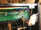
In this iteration of the design, the F-2512 (Connector Circuit board) is crap, but I have put in new molex connectors that plug in to the socket on the bottom side of the board and redid all the traces. I also replaced the molex connectors on each of the F-2507 boards. You can see all of this in the images. I'll put all the new part numbers in a separate message.

1) Is it possible the characteristics of the new transistors have changed the bias setting and are putting out more power than the old ones?
2) I've checked continuity all around F-2512 (on both sides and through the molex connectors) and all is fine. I examined closely for any hairline cracks.
3) Any other ideas anyone can suggest?
4) As an aside, I added fuses to both sides coming from the large capacitors (as others have done) but don't know what amp fuses I should use. One amp fuses seem to be happy, but I'd like to know what they should be by analyzing the circuit.

Thanks for any help provided!
 

Attachments

  • 2e51db8a-f0ba-41fa-b3f0-c648600f9657.jpg
    2e51db8a-f0ba-41fa-b3f0-c648600f9657.jpg
    122.8 KB · Views: 47
  • b2addd01-01aa-48f5-a5ef-66f64771c11a.jpg
    b2addd01-01aa-48f5-a5ef-66f64771c11a.jpg
    137.9 KB · Views: 47
  • faf2d0fc-be09-4dc7-ad70-acbc196a4300.jpg
    faf2d0fc-be09-4dc7-ad70-acbc196a4300.jpg
    165 KB · Views: 47
Register to hide this ad
I'm getting -64V/+64V (vs -68V/+68V) coming from F-2511 (Protection board) and -69V/+69V (vs -65V/+65V) coming from F-2508 (Power Supply board.
Are you sure this is correct? In your photo, the wider traces should be the higher of the two supply voltages.
 
I took it off the DBT and tested again and the thick traces are indeed +67v/-67v and the thin ones (from F-2508) are indeed +69v/-69v with either the two F-2507 boards in or out and the amp is at idle. F-2508 should be putting out +65v/-65v according to the schematic.

F-2508 is only getting -81v/+81v instead of +/- 85v.

What would explain that? Should I be tracking down why the protection board is providing 4v less?
 
DBT would explain why the unregulated voltage appeared low. Line voltage could also affect the voltages coming off the protection board. The regulated voltage is few volts higher than expected, while I don't think it's your immediate problem it would be worth looking into.

Regarding the biasing, it sounds like you’re having to turn the driver transistors on full and the high current is causing them to overheat. Check the emitter resistors on F-2497 by disconnecting the connector at F-2512 and measuring resistance across wires 2 and 4. Expect to see approximately 1.2 Ohms (0.47+0.47 +0.3 test lead resistance)

If that’s good, try measuring the voltages to ground at 28 and 27 on either of the F-2497 Emitter Resistor boards. Start with VR02 set full anti-clockwise and increase to around +500mV and -500mV. That should be enough base voltage for the output transistors to produce a 20mV reading across the emitter resistors.
 
Last edited:
I'd be having a close look at the 4.7Ω series base resistors R35 & R36. ;)

If the unit had blown output or driver transistors those resistors can go open - without showing any signs of it (i.e. burn marks)
 
Last edited:
Check the emitter resistors on F-2497 by disconnecting the connector at F-2512 and measuring resistance across wires 2 and 4. Expect to see approximately 1.2 Ohms (0.47+0.47 +0.3 test lead resistance)

Left channel is 1.6 Ohms and then immediately settles on 1.3 Ohms.
Right channel is 1.6 Ohms and then immediately settles at 1.1 Ohms.
 
If that’s good, try measuring the voltages to ground at 28 and 27 on either of the F-2497 Emitter Resistor boards. Start with VR02 set full anti-clockwise and increase to around +500mV and -500mV. That should be enough base voltage for the output transistors to produce a 20mV reading across the emitter resistors.

Left channel
full counterclockwise
27 = -160mV
28 = +39mV

1/4 from full counterclockwise
27 = -252mV
28 = +125mV

1/2 from full counterclockwise
27 = -522mV
28 = +413mV

3/4 from full counterclockwise
27 = -1.7V
28 = +565mV


Right channel
full counterclockwise
27 = -215mV
28 = -23mV

1/4 from full counterclockwise
27 = -275mV
28 = +45mV

1/2 from full counterclockwise
27 = -502mV
28 = +371mV

3/4 from full counterclockwise
27 = -623mV
28 = +700mV

when I went to full clockwise the right channel burned R33,R34,R35,R36 even without a signal, I didn't even try the left channel.
 
I'd be having a close look at the 4.7Ω series base resistors R35 & R36. ;)

If the unit had blown output or driver transistors those resistors can go open - without showing any signs of it (i.e. burn marks)

R33-R36 are all happy on the left channel. The right channel always burns R33-R36 and I replace them so they are good at least for a while. :)
 
You have enough drive at the driver transistors to cause them to overheat - so plenty. The resistors are OK (at least for a while), including the emitter resistors but you say the output transistors are always cold. Your meter would appear to be OK, and we trust that you are measuring for 20mV (representing the bias current), on the correct pins.

I'll watch the thread, and see where Richard directs you, I'd better not confuse the issue as I don't appear to have the correct schematic.

I see you quoted my WAG. :) - which can't be right as your 4.7Ω resistors can burn.

Check the emitter resistors on F-2497
I can't see this board on my schematic - all I see is F-2509 for emitter resistors. - is there more than one version of the BA-3000 ?
 
Last edited:
You have enough drive at the driver transistors to cause them to overheat - so plenty. The resistors are OK (at least for a while), including the emitter resistors but you say the output transistors are always cold. Your meter would appear to be OK, and we trust that you are measuring for 20mV (representing the bias current), on the correct pins.


I can't see this board on my schematic - all I see is F-2509 for emitter resistors. - is there more than one version of the BA-3000 ?

I am. I see it change when adjusting VR02 and I can get to 20mV but with VR02 all the way clockwise practically. If I keep VR02 to below 1/4, I get sound and everything is fine and null speaker load even with volume all the way to 11 is fine.

There are multiple versions of the boards. Mine are the latest version with the bias transistor on each F-2507 board. The board sandwiched between the heat sinks is F-2509 in the latest revision.
 
I am. I see it change when adjusting VR02 and I can get to 20mV but with VR02 all the way clockwise practically. If I keep VR02 to below 1/4, I get sound and everything is fine and null speaker load even with volume all the way to 11 is fine.
That's interesting. ;)
 
What the heck is a null load and what are you turning all the way up?
Big resistors that simulate the load from a speaker but without destroying your ears.

Dummy load is the correct term actually. Sorry.

I'm cranking it up specifically to make sure under normal operation nothing goes bad especially because I have 4 and 6ohm speakers.
 
Try different right channel outputs, they need a lot of drive to get bias goong for some reason.
 
I am suspicious of your connections from your meter probes to the bias test points or the meter itself. It certainly behaves as if you are turning the bias up way too high.
Sometimes the test points get oxidized and cause false readings. Try this:
1. Power off, connect the meter probes to the bias test points on one channel and measure the resistance. If it doesn't read close to 1 Ohm, scrape the pins and try again. Do the same on both channels.
2. If you got good resistance readings in step one, suspect your meter's accuracy on the mV range. Or possibly you were adjusting to 200mV instead of 20mV, maybe you missed the decimal point location. If you had to crank the adjustment to the max to read 20mV there is no way the driver transistors should be getting hot.
3. Also check TR06 and TR07, just to make sure they are not shorted.
 
1. Power off, connect the meter probes to the bias test points on one channel and measure the resistance. If it doesn't read close to 1 Ohm, scrape the pins and try again. Do the same on both channels.

Am I testing F-2507 or F-2497? With F-2507 pulled out and probing the correct pins I am getting 0 ohm but testing F-2497 on the same pins as richard had me do, I am getting the below... (hopefully that makes sense.... i'm testing for resistance across the exact same pins as testing bias with F-2507 in the slot but with power off).

Check the emitter resistors on F-2497 by disconnecting the connector at F-2512 and measuring resistance across wires 2 and 4. Expect to see approximately 1.2 Ohms (0.47+0.47 +0.3 test lead resistance)

Left channel is 1.6 Ohms and then immediately settles on 1.3 Ohms.
Right channel is 1.6 Ohms and then immediately settles at 1.1 Ohms.

I did replace all the molex connectors, btw, because they were a mess. corrosion and weak contacts as you point out.

I'll check 200mV vs 20mV after I replace the burned transistors on the right channel again as well as look at T06 and T07 again. I agree with you, it just seems like the bias is too high. My multimeter is nothing fancy.
 
Back
Top Bottom