Hi all,
I thought I'd post these extended notes for posterity sake and hope they are of use to someone else that is in the process of rebuilding this type of receiver. I didn't take the time to include every hoop and hurdle. I also note that I'm no expert but I am willing to go down just about every rabbit hole. Apologies in advance if someone finds my approach an anathema (or a bone-headed hack).
One recommendation I have is to make sure you have some good basic analytical tools, a decent desoldering tool (I broke down and bought a Hakko....and, in the end, it was well worth it), and a temperature controlled solder station.
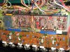
As received most everything tested was working. As per usual the pots were scratchy, there was mild hum and hiss and the tuner alignment had drifted. After almost 50 years there are components that should be replaced. While many of the electrolytic caps tested fine, a small but significant number had values well out of the stated capacitances plus high ESR and loss values (especially those rated at 3.3uf or less). At this point experience suggests that replacing all of them is a good way to avoid piecemeal problems going forward.
In the end I wound up replacing all of the electrolytic caps (on each and every board and often with those having higher ratings). I can't get a straight answer on what caps work best (complaints with respect to Elna Silmic II and Nichicon Muse, among other, are often posted) so I generally default to Nichicon fine gold.
Most of the coupling caps in the audio signal path (both electrolytic and tantalum with capacitances at or below 2.2uF) were replaced with Wima or Panasonic polypropylene equivalents. In two cases (that of the phono and CD-4 decoder boards) there wasn't always physical space on the board to allow for this substitution. Nichicon PW (105 C) and VP (bipolar) caps were used in the power supply board. In all other boards either Nichicon FG (fine gold) or ES (bipolar muse) were typically used (otherwise low ESR audio Nichicon KL or Elna Silmic II were substituted). The two axial caps were replaced using one Sprague and one Vishay cap. For the three main power/filter caps long-life EPCOS caps were used. Transistors known to age badly (e.g., the 2SC1312) were replaced (tone, phono, CD-4 demodulator, SQ matrix boards, driver board) and, where needed, with matched KSC1485 or KSA992 pairs. Sixteen transistors on the driver board were replaced. All told over 50 transistors were exchanged. The trim pots on the driver board were replaced with Bourn cermets. All incandescent lamps (29 in total!) except the tuner dial lamp, were replaced with LEDs. These lamps include a SMD rectifier in their circuit so that there is no annoying 60 Hz flicker.
Specific repair notes:
1. Two of the four AM/FM backlight fuse lamps were intermittent (a known issue with Sansui receivers). This was remedied by remelting the solder on the fuse lamp clip bases. With the LED upgrade the thermal stress on the clip base solder joints should be eliminated.
2. The stereo multiplex portion of the tuner was far out of alignment. You can spend a lot of money on FM alignment components but I have found a number of tricks that will all one to align the FM section on the cheap. A good set of nylon alignment tools is a must. Between a cell phone function generator app, a small USB FM stereo transmitter, good digital scope and handheld DMM there is a lot one can achieve as long as one isn't too concerned with getting the signal level calibrations exactly to spec. Make sure you document the position of the trim pots, trim caps and trim inductors beforehand or there can be real trouble. I do note that I do use a Leader distortion meter to make sure that the alignment process doesn't create problems in the audio quality.
3. Using headphones a 60 Hz hum could easily be heard when the volume was set to a minimum. Oddly it would first decrease to a minimum as the volume was increased and then smoothly increase with volume. With the recap of the power & protection board this issue was eliminated. The board looked as if errors may have been made in its original assembly. Two capacitors did not match the circuit schematic and were underrated, one in its capacitance and one in its voltage and capacitance rating. The aforementioned odd behavior ended when testing the unit after the two proper rated caps were installed (along with a few others). There was also a spurious electrolytic cap mounted which was undocumented in the service manual schematic. Although the reason for its inclusion is unclear it was retained and replaced with a new cap.
4. A small bit of 60 Hz hum on the front left channel, independent of volume, was still present after item 3. After replacing four caps on the driver board and the two main amplifier power caps this issue was resolved.
5. When the burned out CD-4 bulb was replaced with a red LED it was then observed to be always lit. This problem was traced to a fault in the adhoc upgrade patch (a factory original for the QRX-7500A) on the CD-4 demodulator board (which from what I could tell more amplification was needed to adequately drive the original incandescent bulb). With an LED the original circuit, using a KSA992 instead of the 2SC933 (and connecting an 82ohm current limiting resistor to the base lead), worked as desired when tested with a 30 kHz carrier signal. One of the added resistors from the ad-hoc modification was retained so that the CD-4 level pot worked as stated in the nominal 1-10mV range for the 30kHz carrier signal. See the CD-4 test below for full details.
6. Cold solder joints were found which affected the receiver's functioning in a few places.
7. At this point there was more residual circuit hum if the AC plug has particular orientation in the AC socket. The blade which should be plugged into the neutral socket (i.e., the wider one in an ungrounded 2 pin socket) has a small black ring to indicate the proper polarity. Alternatively a polarized plug can be substituted for the original. At minimum volume any residual background hum, through closed ear headphones, was very difficult to discern (and then only on the front channels). This appears to be a design limitation because of the tone board placement. After adding an additional shielding plate over the tone board followed by replacing 16 transistors on the amp driver board this issue seems to be gone altogether.
Here is the link to the list of transistors I look for replacing:
https://audiokarma.org/forums/index...ilure-prone-whatever-and-replacements.731653/
8. SQ dial settings: A true stereo signal is necessary. It is important to note that for the two SQ boards to work properly they require a near perfect 25V output from the power supply board. When first switched on the value is closer to 24.5V and then, over some five minutes, drifts up to 25.00V (+/-.01 V). During the first minute or so the audio behavior of the SQ circuit may change.
The response of the SQ Matrix mode is shown in the Youtube link
(note that the blend resistors have been retained). The simulated test tone sequence is Center Front - Left Front – Center Left – Rear Left – Center Rear – Right Rear – Center Right – Right Front – Center Front
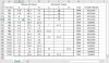
The nominal level read outs (LF/RF/LR/RR) are:
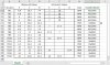
-2/ -2/-18/-18 Center Front
0/-18/-10/-20 Left Front
-4/-17/ -7/-13 Center Left
-8/-20/ -2/-18 Rear Left
-13/-13/ -3/ -3 Center Rear
-20/ -9/-16/ -2 Right Rear
-12/ -6/-15/ -6 Center Right
-18/ 0/-20/-10 Right Front
-2/ -2/-18/-18 Center Front
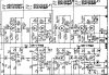
***In addition it must be noted that the F-2047 Vario Matrix board held some surprises. The service manual schematic does not match the actual physical board circuitry in numerous places and, in addition, the circuit board itself is mismarked in at least two locations (transistor pinouts). I've seen similar problems in other service manuals....caveat emptor.
9.. Offset and bias adjusted to service manual specifications
10. Tuners aligned for improved reception and, in the case of FM, less distortion and much better stereo signal separation. See the above item.
Final notes:
1. All four amplifier stages run at the 16V_rms rating (32 wpc into an 8 ohm load) using a 1kHz test tone. They begin clipping just a bit below 17 V_rms (which doesn't give a lot of headroom). The THD was also measured at 1kHz and all four channels were well below the stated specifications.
2. Both AM and FM tuners work well. The FM tuner has excellent sensitivity and very good selectivity. Note that the left FM stereo signal is a tiny bit stronger than that of the right (discerned using a 1kHz test tone broadcast the difference is just about one unit, presumably 1db, on the audio level meters). This difference was present before servicing the tone board. There are no output pots on the tuner board to allow for additional fine adjustment.
3. Both the front and rear low filter switches exhibit a very slight pop when disengaged.
4. This is apparently a late version of the QRX-7500 as a few of the boards are not included in the service manual but, rather, show up in that of the QRX-7500A.
5. Only the left phono input is configured to respond to a 30kHz quadraphonic carrier signal.
6. One very annoying characteristic in this QRX-7500 is that it only has an FM auto dial setting. Thus a radio station with a modest FM signal strength can generate stereo reception with annoying hiss. To compensate, most receivers allow one to switch to FM mono reception. To enable this function in this Sansui custom wiring has been added which goes from the FM muting off switch to the tuner board. Now, when the FM muting off switch is engaged (i.e., disabling FM muting), the FM tuner now simultaneously switches into FM mono reception.
7. The LED lamp power supply (just a simple transformer tap) is unregulated and so the voltage does vary with the actual number of lamps used. LED luminosity can be very sensitive to small changes in the voltage. Thus some variations are observable when switching the number of lamps that are energized.
8. Some residual scratchiness of the volume pot can be discerned if it is turned quickly to high volume and there is no audio source.
Lighting notes: Getting the lighting to match that of the original proved challenging. The AM/FM tuner display was exceedingly dim even when all the incandescent fuse lamps were working. Both daylight and warm white LEDs were tested and, of the two, daylight lamps worked best. Even then the AM/FM display wasn't quite as bright as I would have preferred (still a big improvement). As a consequence the green of the AM/FM display is a bit purer in its tone and the 0...10....to...100 scale below is a bit more yellow than in the original. The meter displays are much brighter as well but still a fairly close color match. In addition to the backlight every meter also includes two small bulbs (off the field of view) for illuminating the meter needle base when there is no room light. Most of these had burnt out and there was extensive darkening of the surrounding plastic from the heat build up. The LED replacements are a bit more yellow in tone and have been adjusted in brightness so they don't overwhelm the black meter face with unwanted glare. For the two phono LED bulbs, green LEDs were substituted for the standard yellow-amber. With this LED upgrade the maximum power used when in idle drops from something close to 60 watts to between 25 and 27. The reason it is still relatively high (as compared to other receivers) is that all the electronic boards are fully energized when the receiver is on.
CD-4 test notes:
1. Initially a 30kHz pilot signal was found to properly illuminate the CD-4 lamp. Without this lamp being lit the full CD-4 decoder circuit will not function.
Although I do not have a quadraphonic test disc set up it is possible to test the decoder with a CD-4 needle drop .flac recording and a USB sound card with a sufficiently high frequency response. I used an ASUS Xonar U7 MKII which has a 192kHz DAC (and is said to output up to 55kHz, well above the 20-45kHz range employed in CD-4 disc recordings). At first I tried a claimed CD-4 test record recording but that recording did not work as intended. As a result I went to the trouble of fully simulating (using the computer program Partsim which I believe employs Spice as the simulation engine) one channel of the entire CD-4 decoder circuit (except the FM decoder chip) that resides on the CD-4 and phono boards. All of the circuit elements checked out in terms of the DC voltages and AC gain measured at various test points indicating that nothing was amiss. My scope has a built in FFT function which made it easy to see the FM encoded signal before the demodulator chip. Interestingly one of tested subcircuits I prototyped gave bogus results in the simulated transient response. I guess you have to take everything with a small grain of salt. The good news is that even if you don't have the background to look at a circuit diagram and figure out the proper behavior the simulation software goes a long way to ramping one up the learning curve.
2. Thereafter I downloaded a short Marvin Gaye CD-4 recording "Mercy, mercy, me.flac" and this file ran through the decoder just fine. Although the front and rear channels have about the same average signal strength on the Sansui meters, one can look more carefully by directly visualizing the left (or right) front and left rear outputs (accessible on the phono board) on the oscilloscope. The actual scope traces, seen in a Youtube video
(yellow for front and cyan for rear) are significantly different (and indicated by the difference plot in a poorly rendered purple). One can also audibly hear that sound is different (not on the video).
3. There was one important observation. In moving from a stereo to the quadraphonic switch setting there is a noticeable drop in the signal level so that the small level adjust knob needed to be increased (in this case to 10). This is due to an additional line resistor in the audio path on the phono board which drops the level. Adjusting things proved a bit tricky because one also needs to keep from saturating the FM decoder chip (via the CD-4 level knob).
4. Supplement for the user manual. A. CD-4 level knob adjusts the total signal strength, including the 30kHz pilot signal, just before the FM decoder chip. Thus it will also modify the "front-back" signal level. The Left and Right stereo separation knobs adjust the signal level of the respective "front+back" tracks.
That is all for now.
As I said, I hope this helps.
I thought I'd post these extended notes for posterity sake and hope they are of use to someone else that is in the process of rebuilding this type of receiver. I didn't take the time to include every hoop and hurdle. I also note that I'm no expert but I am willing to go down just about every rabbit hole. Apologies in advance if someone finds my approach an anathema (or a bone-headed hack).
One recommendation I have is to make sure you have some good basic analytical tools, a decent desoldering tool (I broke down and bought a Hakko....and, in the end, it was well worth it), and a temperature controlled solder station.
As received most everything tested was working. As per usual the pots were scratchy, there was mild hum and hiss and the tuner alignment had drifted. After almost 50 years there are components that should be replaced. While many of the electrolytic caps tested fine, a small but significant number had values well out of the stated capacitances plus high ESR and loss values (especially those rated at 3.3uf or less). At this point experience suggests that replacing all of them is a good way to avoid piecemeal problems going forward.
In the end I wound up replacing all of the electrolytic caps (on each and every board and often with those having higher ratings). I can't get a straight answer on what caps work best (complaints with respect to Elna Silmic II and Nichicon Muse, among other, are often posted) so I generally default to Nichicon fine gold.
Most of the coupling caps in the audio signal path (both electrolytic and tantalum with capacitances at or below 2.2uF) were replaced with Wima or Panasonic polypropylene equivalents. In two cases (that of the phono and CD-4 decoder boards) there wasn't always physical space on the board to allow for this substitution. Nichicon PW (105 C) and VP (bipolar) caps were used in the power supply board. In all other boards either Nichicon FG (fine gold) or ES (bipolar muse) were typically used (otherwise low ESR audio Nichicon KL or Elna Silmic II were substituted). The two axial caps were replaced using one Sprague and one Vishay cap. For the three main power/filter caps long-life EPCOS caps were used. Transistors known to age badly (e.g., the 2SC1312) were replaced (tone, phono, CD-4 demodulator, SQ matrix boards, driver board) and, where needed, with matched KSC1485 or KSA992 pairs. Sixteen transistors on the driver board were replaced. All told over 50 transistors were exchanged. The trim pots on the driver board were replaced with Bourn cermets. All incandescent lamps (29 in total!) except the tuner dial lamp, were replaced with LEDs. These lamps include a SMD rectifier in their circuit so that there is no annoying 60 Hz flicker.
Specific repair notes:
1. Two of the four AM/FM backlight fuse lamps were intermittent (a known issue with Sansui receivers). This was remedied by remelting the solder on the fuse lamp clip bases. With the LED upgrade the thermal stress on the clip base solder joints should be eliminated.
2. The stereo multiplex portion of the tuner was far out of alignment. You can spend a lot of money on FM alignment components but I have found a number of tricks that will all one to align the FM section on the cheap. A good set of nylon alignment tools is a must. Between a cell phone function generator app, a small USB FM stereo transmitter, good digital scope and handheld DMM there is a lot one can achieve as long as one isn't too concerned with getting the signal level calibrations exactly to spec. Make sure you document the position of the trim pots, trim caps and trim inductors beforehand or there can be real trouble. I do note that I do use a Leader distortion meter to make sure that the alignment process doesn't create problems in the audio quality.
3. Using headphones a 60 Hz hum could easily be heard when the volume was set to a minimum. Oddly it would first decrease to a minimum as the volume was increased and then smoothly increase with volume. With the recap of the power & protection board this issue was eliminated. The board looked as if errors may have been made in its original assembly. Two capacitors did not match the circuit schematic and were underrated, one in its capacitance and one in its voltage and capacitance rating. The aforementioned odd behavior ended when testing the unit after the two proper rated caps were installed (along with a few others). There was also a spurious electrolytic cap mounted which was undocumented in the service manual schematic. Although the reason for its inclusion is unclear it was retained and replaced with a new cap.
4. A small bit of 60 Hz hum on the front left channel, independent of volume, was still present after item 3. After replacing four caps on the driver board and the two main amplifier power caps this issue was resolved.
5. When the burned out CD-4 bulb was replaced with a red LED it was then observed to be always lit. This problem was traced to a fault in the adhoc upgrade patch (a factory original for the QRX-7500A) on the CD-4 demodulator board (which from what I could tell more amplification was needed to adequately drive the original incandescent bulb). With an LED the original circuit, using a KSA992 instead of the 2SC933 (and connecting an 82ohm current limiting resistor to the base lead), worked as desired when tested with a 30 kHz carrier signal. One of the added resistors from the ad-hoc modification was retained so that the CD-4 level pot worked as stated in the nominal 1-10mV range for the 30kHz carrier signal. See the CD-4 test below for full details.
6. Cold solder joints were found which affected the receiver's functioning in a few places.
7. At this point there was more residual circuit hum if the AC plug has particular orientation in the AC socket. The blade which should be plugged into the neutral socket (i.e., the wider one in an ungrounded 2 pin socket) has a small black ring to indicate the proper polarity. Alternatively a polarized plug can be substituted for the original. At minimum volume any residual background hum, through closed ear headphones, was very difficult to discern (and then only on the front channels). This appears to be a design limitation because of the tone board placement. After adding an additional shielding plate over the tone board followed by replacing 16 transistors on the amp driver board this issue seems to be gone altogether.
Here is the link to the list of transistors I look for replacing:
https://audiokarma.org/forums/index...ilure-prone-whatever-and-replacements.731653/
8. SQ dial settings: A true stereo signal is necessary. It is important to note that for the two SQ boards to work properly they require a near perfect 25V output from the power supply board. When first switched on the value is closer to 24.5V and then, over some five minutes, drifts up to 25.00V (+/-.01 V). During the first minute or so the audio behavior of the SQ circuit may change.
The response of the SQ Matrix mode is shown in the Youtube link
The nominal level read outs (LF/RF/LR/RR) are:
-2/ -2/-18/-18 Center Front
0/-18/-10/-20 Left Front
-4/-17/ -7/-13 Center Left
-8/-20/ -2/-18 Rear Left
-13/-13/ -3/ -3 Center Rear
-20/ -9/-16/ -2 Right Rear
-12/ -6/-15/ -6 Center Right
-18/ 0/-20/-10 Right Front
-2/ -2/-18/-18 Center Front
***In addition it must be noted that the F-2047 Vario Matrix board held some surprises. The service manual schematic does not match the actual physical board circuitry in numerous places and, in addition, the circuit board itself is mismarked in at least two locations (transistor pinouts). I've seen similar problems in other service manuals....caveat emptor.
9.. Offset and bias adjusted to service manual specifications
10. Tuners aligned for improved reception and, in the case of FM, less distortion and much better stereo signal separation. See the above item.
Final notes:
1. All four amplifier stages run at the 16V_rms rating (32 wpc into an 8 ohm load) using a 1kHz test tone. They begin clipping just a bit below 17 V_rms (which doesn't give a lot of headroom). The THD was also measured at 1kHz and all four channels were well below the stated specifications.
2. Both AM and FM tuners work well. The FM tuner has excellent sensitivity and very good selectivity. Note that the left FM stereo signal is a tiny bit stronger than that of the right (discerned using a 1kHz test tone broadcast the difference is just about one unit, presumably 1db, on the audio level meters). This difference was present before servicing the tone board. There are no output pots on the tuner board to allow for additional fine adjustment.
3. Both the front and rear low filter switches exhibit a very slight pop when disengaged.
4. This is apparently a late version of the QRX-7500 as a few of the boards are not included in the service manual but, rather, show up in that of the QRX-7500A.
5. Only the left phono input is configured to respond to a 30kHz quadraphonic carrier signal.
6. One very annoying characteristic in this QRX-7500 is that it only has an FM auto dial setting. Thus a radio station with a modest FM signal strength can generate stereo reception with annoying hiss. To compensate, most receivers allow one to switch to FM mono reception. To enable this function in this Sansui custom wiring has been added which goes from the FM muting off switch to the tuner board. Now, when the FM muting off switch is engaged (i.e., disabling FM muting), the FM tuner now simultaneously switches into FM mono reception.
7. The LED lamp power supply (just a simple transformer tap) is unregulated and so the voltage does vary with the actual number of lamps used. LED luminosity can be very sensitive to small changes in the voltage. Thus some variations are observable when switching the number of lamps that are energized.
8. Some residual scratchiness of the volume pot can be discerned if it is turned quickly to high volume and there is no audio source.
Lighting notes: Getting the lighting to match that of the original proved challenging. The AM/FM tuner display was exceedingly dim even when all the incandescent fuse lamps were working. Both daylight and warm white LEDs were tested and, of the two, daylight lamps worked best. Even then the AM/FM display wasn't quite as bright as I would have preferred (still a big improvement). As a consequence the green of the AM/FM display is a bit purer in its tone and the 0...10....to...100 scale below is a bit more yellow than in the original. The meter displays are much brighter as well but still a fairly close color match. In addition to the backlight every meter also includes two small bulbs (off the field of view) for illuminating the meter needle base when there is no room light. Most of these had burnt out and there was extensive darkening of the surrounding plastic from the heat build up. The LED replacements are a bit more yellow in tone and have been adjusted in brightness so they don't overwhelm the black meter face with unwanted glare. For the two phono LED bulbs, green LEDs were substituted for the standard yellow-amber. With this LED upgrade the maximum power used when in idle drops from something close to 60 watts to between 25 and 27. The reason it is still relatively high (as compared to other receivers) is that all the electronic boards are fully energized when the receiver is on.
CD-4 test notes:
1. Initially a 30kHz pilot signal was found to properly illuminate the CD-4 lamp. Without this lamp being lit the full CD-4 decoder circuit will not function.
Although I do not have a quadraphonic test disc set up it is possible to test the decoder with a CD-4 needle drop .flac recording and a USB sound card with a sufficiently high frequency response. I used an ASUS Xonar U7 MKII which has a 192kHz DAC (and is said to output up to 55kHz, well above the 20-45kHz range employed in CD-4 disc recordings). At first I tried a claimed CD-4 test record recording but that recording did not work as intended. As a result I went to the trouble of fully simulating (using the computer program Partsim which I believe employs Spice as the simulation engine) one channel of the entire CD-4 decoder circuit (except the FM decoder chip) that resides on the CD-4 and phono boards. All of the circuit elements checked out in terms of the DC voltages and AC gain measured at various test points indicating that nothing was amiss. My scope has a built in FFT function which made it easy to see the FM encoded signal before the demodulator chip. Interestingly one of tested subcircuits I prototyped gave bogus results in the simulated transient response. I guess you have to take everything with a small grain of salt. The good news is that even if you don't have the background to look at a circuit diagram and figure out the proper behavior the simulation software goes a long way to ramping one up the learning curve.
2. Thereafter I downloaded a short Marvin Gaye CD-4 recording "Mercy, mercy, me.flac" and this file ran through the decoder just fine. Although the front and rear channels have about the same average signal strength on the Sansui meters, one can look more carefully by directly visualizing the left (or right) front and left rear outputs (accessible on the phono board) on the oscilloscope. The actual scope traces, seen in a Youtube video
3. There was one important observation. In moving from a stereo to the quadraphonic switch setting there is a noticeable drop in the signal level so that the small level adjust knob needed to be increased (in this case to 10). This is due to an additional line resistor in the audio path on the phono board which drops the level. Adjusting things proved a bit tricky because one also needs to keep from saturating the FM decoder chip (via the CD-4 level knob).
4. Supplement for the user manual. A. CD-4 level knob adjusts the total signal strength, including the 30kHz pilot signal, just before the FM decoder chip. Thus it will also modify the "front-back" signal level. The Left and Right stereo separation knobs adjust the signal level of the respective "front+back" tracks.
That is all for now.
As I said, I hope this helps.
Last edited: