• The move to the new server is done. There are some software and database maintenance updates in process. This has us passing the hat around to help out. We appreciate any donations. Seriously, even a dollar helps. The payment page may be found here - https://www.audiokarma.org/support.html

Sony TA-F6B Integrated Amp IC issue.

zebulon1

Retired finally and having a blast on the bench
Subscriber
The amp had the right channel blown.
Repaired all that.
It needs the Linear Amp IC Sony "CX171" 14 pin DIP to finish the work.
I can't find an exact replacement.
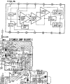
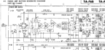
Does anyone have any info on a replacement? The image below is a similar chip but the seller say's it wont work. No datasheets available.
Swapping the chips was a gamble but it proved a good troubleshooting technique. Somehow its not causing a full power on bias. I think it already did that?

Screenshot 2024-01-11 2222.png

1704995764126.png

Screenshot 2024-01-11 100419.png
 
Register to hide this ad
Hi, i have on my workbench a SONY TA-F6B with two CX171 damaged, the bias adjustment don't work and after 10W and above the amplifier distort the signal heavy in the upper sine wave. I measured with the sope and the circuit on both channels have the same issue. After some research i found that this is a common problem with these circuits, and because is no longer available i step in and take the oportunity to design from scrach a replacement made by discrete components(diodes, resistors, transistors, etc).
I am aware that this work could help others guys like you and me that search an replacement to CX171; the problem is harder AND UGLY because of lack of documentation I.E. the datasheet.
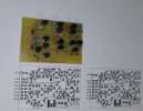
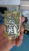
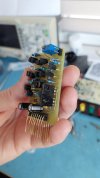
As i say, until now i designed and tested a promising DROP-IN replacement in LTSPICE that work beautiful, i have build the circuit board and assembled in proportion of 90%. Is not tested yet in practice, i think this week i will do. Is like a small PCB with headers that go in the same place of the original circuit. I will attach a picture with the board . After testing with signal generator and oscilloscope with a 8R load and validate the schematic, i will post here for free thr design files, schematic and simulation files for anyone is interested to revive a dead sony with cx171. In the simulation i have tested the "replacement" using all the sony schematics that use this circuit: TA-F4A, TA-515, TA-F60 and behave perfect , like an ic.
I will update this when i will end the work.

20240512_002537.jpg
 
Very nice. I like the idea of using discrete parts. Hopefully it works out for you. Working on Sony equipment can be difficult sometimes due to the use of proprietary parts with little or no data for these parts. Some of them are acually more commonly known parts just with Sony's part numbers on them.
 
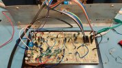
Work in progress. Of course, simulatoon is diffrent from reality. The designed replacement module don't work too good, i had to remove it and i took a flat cable from amplifier board to the breadboard and make the schematic of the cx171 replacement on breadboard, its easyer to adjust components and make measurements in this way. The good news is that i have promising results! But i have to adjust the quiscent current circuit and some transistor biasing isue.
1000029930.jpg1000029929.jpg
 
Hi guys, i have good news and a funny story! The good news is that i have succesfully finish the CX171 replacement schematic, the funny story is that my CX171 circuits are in fact good!, the problem with distorted signal on the output on the positive rail is beacause a cheap transistor in the overcurrent section of the amplifier was partial shorted, and yes, it was the same transistor on both channels, that transistor is named Q304 (left channel) and Q354 on the right channel. A curious thing is that the transistor was another type than the one in the schematic, and was original, never replaced.
Soooo, you guys are the only beneficiars of my work. And anyone who find this thread.
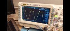
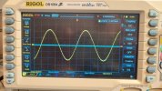
So lets get started: here is the picture with the distorted output on the positive rail:​
Screenshot_20240617_133405_Gallery.jpg

That Q304 transistor was the bad guy here. But anyway, the good news is that i can compare the replacement schematic with a working CX171! Here is the test with original CX171:​
20240615_001529.jpg
20240615_001531.jpg
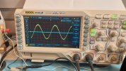
I want to mention that the test is done with 20KHZ sine wave input and the output is conected on a 8R 100W resistor as load. Iou can see a little noise on the upper wave because of parasitic inductance and lack of decoupling of CX171 that are mounted on bread board.
Next are the pictures with the replacement schematic inserted instead of CX171:

20240615_000936.jpg20240615_001210.jpg​
So the conclusion is that the replacement act like the original CX171. In my opinion i think is better in terms of noise. Also it have exactly the same gain, i have the same amplitude level between 20Hz and 20 Khz as the original circuit.
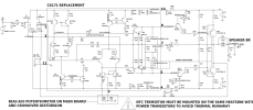
Now the schematic:
CX171 REPLACEMENT MODULE.png
The schematic is published here in pdf format for better resolution, i also put the LTSPICE schematic for anyone who want to play and make simulations with LTSPICE. I also uploaded the pcb file for circuit board, is designed by me in diptrace? It have a single layer with a few jumper wires and made only with trh components(trough-hole).

Now the comments:
  • First, this is a design that can be improved. I am aware that i am not a master in electronics design, but what i offer is free and a working solution (and tested) in this problem with obsolete CX171. I know how to design and solder smt boards, but i want that this design to be easy to make at home by peoples that don't like smd's.
  • The replacement module is in the dotted area in the schematic, with coresponding pins printed.
  • Another thing: i have used a 10k termistor for eliminate the danger of thermal runaway. The original CX171 didn't have this control, at least i am not aware of that. The termistor must be mounted on the same heatsink with the power transistors , as much as close to them.
  • I have tested the amplifier at full load until the heatsink has too hot to touch and the quiscent current was under 120mA. Also the quiscent current is around 100mA when the amplifier is cold at room temperature.
  • In the schematic, i had to insert C2 and R30 for stability at high levels and ultrasonic frequencyes.
  • The original bias potentiometer from the mainboard of the amplifier RT302 have a diffrent purpose: to eliminate crossover distorsions. This must be adjusted at a very low signal input and with 8r load conected at the output, oscilloscope conected across load. Very low signal is about 0.01V 1Khz. The adjusting must be done in conjunction with the offset potentiometer RT301(dc ballance) alternative.(RT301 - RT302-RT301 again, RT302); until you have a nice sine wave on the scope , qith quiscent current below 60mA.
  • The R53 from the replacement module set the quiscent current up to 100mA.
  • In reality the distorsions of the amplifier is smaller than in the simulation, because the simulation don't have the real world components and i had to improvise.
  • BC556 and BC546 is used in the simulation, i guess it works ok in the practice, but i will do the tests with BC550 and BC560, have low noise.
  • instead of NMOS BSS123 from simulation i have used BS170. Is not necesary to mount on the heatsink, only the termistor.
  • The type of termistor is in attachments, as pdf.
  • The D4 is a blue LED, and act as a analog level shifter. It could be replaced with 5 diodes 1N4148 ; The voltage drop across him are around 2.3V.
  • Of course, like any simetrical audio amplifier, all the transistors must be complementary and with equal current gain as possible. For example, don't mix BC546B with BC546C or A.
  • D1 and D12 ARE 9.1V zenner diodes and act as a shunt regulator. The whole board instead of NMOS ,Q12,Q14, Q6,Q28 works under 18V. But transistors mentioned before must be over 60V C-E.
  • Q14 and Q28 make all the effort . Despite their 1.4W power disipation, they do not heat much and is not necesary to mount on a heatsink, but i designed the pcb in that way for allow this if necesary.

In the next post i will make the replacement pcb and mount in the amplifier and make the final pictures with final tests, I want to make some distorsion and frequency response tests on my computer, using the audiocard as analog IO.
​
Thats it for now, i will see next time! Greetings from ROMANIA!​
 

Attachments

Last edited:
Hello friends, yesterday i made the pcb in my home :
1000030537.jpg
I always make my own pcb by toner transfer method. After transferring the components from breadboard to pcb, cut the terminals and soldering the module is ready:
1000030715.jpg1000030717.jpg1000030722.jpg1000030730.jpg1000030734.jpg1000030738.jpg
Now, i will solder the module in place of CX171:
1000030752.jpg1000030755.jpg1000030760.jpg
Here you can see the 10k ntc thermistor mounted on the heatsink glued inside of round crimp pin. The best way was to mount the ntc directly on the collector of one of final transistors, but because of collector is conected trough the speaker output, at high volumes the amplifier distort the signal because of parasite capacitor coupling between ntc sesnor and final transistor. So the solution was to ground the metal plate of the ntc and isolate , or, mount on the heatsink , witch is already to ground. I prefered the second solution, is more simple. The only disadvantage is that is a lag of several seconds until heat from power transistor go in to the ntc to regulate the quiscent current .
In reality is not that bad. After a hard stres at 100% power, right after turning down the volume, the quiscent current of the amplifier is around 150mA, and in a few seconds go to around 100mA. I am happy with this result. It is ok i my opinion.​
Today i have done some testing, the amplifier was powered on my diy lab power supply (smps regulated and constant current), at 50V +/-, yes is noisy, i know. Maibe in the future i will buy a proper one. I have connected my 8 ohm 100w resistor as load, and conected the signal generator ( its dds, i know, maybe i the future i will buy a proper one, but is stable and constant in amplitude in audio range).​
In the next post i will attach the result pictures, here i have reached the 10 pictures limit and i can't upload any picture anymore.
 
Now the pictures:
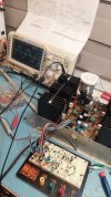
1000030761.jpg
You can see the dummy load in the right of the amplifier. Is a 15cm resistor. 5cm diameter.. but fo hot in a minute at full load.
Here is the amplifier at 1khz right before clipping.:
1000030763.jpgAnd here is the 20khz signal at the output , the same , right before clipping:
1000030764.jpg As you can see, the signal is ok, simetric and not distorted. I am happy with this result.
For science, here are a picture where the amplifier go in to clipping because of overdrive:​
1000030765.jpg​
As a personal observation the original CX 171 do rhe same clipping in these conditions. Next, in the next week i will try to make a sweep with "REW" on my pc, from 20hz to 20Khz , to test the frequency response and Thd. Just for science. I am curious to make a comparison between my replacement module and the original SONY CX171 circuit.
You may ask why i don't use the superdiode transistor as a sensing device for thermal runaway and choose a sntc to do that.... Well, because if i will heat up the transistor, quiscent current of the amplifier goes up! And this is exactly the opposite of what i want! By using an ntc placed in the right spot when the themperature goes op, the quiscent current goes down!​

The spot of the R53 that adjust the quiscent current is very specific: if in time goes bad, in general the trim pots increase in value or go completely interrupted. Well, in this cade the quiscent current go down at minimum. To protect thenpower transistors in case of this failure.

Until next time, greetings from ROMANIA! Bye!...​
 
Last edited:
Hahahaha -- the first post made me laugh ... in the block diagram for the ic ...it says current "miller" ... hehehehe ... Current mirrors ...and miller effect rolled into one. :thumbsup:

This is excellent work ... the best I have done is back engineer STK's and make own pcb with descrete devices.
In our workshop this level of work, excellent though it is, would not be economically viable to do.

How do you not get intermittency throrugh breadboard.? . When ever I use small signal devices in breadboard , I'm always fighting internittent connections.
 
I did change VFET 5650 into a standard MosFet version - I designed so I could use 2sj56 and 2sk176 devices. I took inspiration from Hafler DH220 made some changes and improvements to accomodate the lower voltage rails. I found damping factor - thermal efficiency was improved + being able to obtain FETs more easily.

Vfet.jpg


FET -  - 5650 Sony.jpg
 
Last edited:
Some excellent work here (though I don't think anyone in this thread is doing the work thinking about the economics of same).
I'll just hope the Sony (who once upon a time had its own fabs in San Antonio & Austin, TX - a friend worked in them in the '80s) ICs in my TA-F6B don't give up.
 
Thanks for the kind words! The breadboard i use is WishBoard 502-L, (see picture) .
1000030226.jpg
It have round holes and round contacts inside. I have them( 2 of them) from 2012 and are working until this day without problems. I misbehave with them and abused with very thin terminals up to 0.9mm . I even designed power smps on them! No problems whatsoever...
 
Hello again, i have the final results. Iesterday i have tested the SONY TA-F6B amplifier with my PC, using REW program, the line out of the soundcard goes in to the imput of the amplifier, and the output of the amplifier witch is connected to 8R load goes trough an atenuator(for not blowing up my soundcard with 90Vpp) to the line in of PC.
Before the testing, i calibrated the sound card to give a flat response over audio range 20Hz-20Khz. This is done conecting the soundcard in loopback mode, R channel line out to L channel line in.​
So first i had installed the CX171 replacement board, do the testing, then replace the board with original SONY CX171 circuit,(and re make the dc bias and current adjustments acording to service manual) and most impornant thing: with same setup, same settings, same PSU, i made the the same tests.
I want to do this way because i know of the limitations of the testing: long wires, bad shielding(i have a very noisy power supply and the amplifier is out from the metal case), not to mention that i have the on board sound card, a decent one ( 24 BIT at 192Khz ), but not professional for audio testing. In loopback mode , the THD is around 0.02%, so i have a baseline of my soundcard and wiring.​
Regarding the tests , i have done two tests, a sweep from 20hz to 20Khz to see the frequency response, and THD. All the tests are done with the load conected at the output and at full power, the oscilloscope measure during tests 88Vpp at the output of amplifier. If i go over 90Vpp, the amplifier go in to clipping.
Here are the results: First, the replacement board:
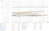
SWEEP AT 88VPP REPLACEMENT.png
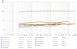
So we see that over the audio domain, i have a diffrence of 0.4db ,but i see that i have an increase of signal at high frequencyes.I think is from C2 capacitor that i put for stability of the amplifier in case of overdrive at ultrasonic frequencyes.

Now the THD:
THD AT 88VPP REPLACEMENT.png
The THD at 1Khz is reported as 0.952% With is acceptable, but it could be better and i think it could be improved. I suspect the same capacitor.

Next, i removed the board i made and solder the original SONY CX171 circuit, do the trim pots adjustments to current and dc bias and do the same tests, with the same settings:

20240627_205146.jpg


SWEEP AT 88VPP ORIGINAL CX171.png
You see the sweep, i have an atenuation at higher frequencyes, but the diffrence is around 0.3db witch is ok, similar with my board but in opposite direction.
Now the THD:​
​
THD AT 88VPP ORIGINAL CX171.png​
Here is a big pleasant surprise! THD at 1khz is reported as 0.087% ! Much lower! So SONY original IC is better! This was to be expected! I am not an SONY engeneer!;)​
That's why i want to do the comparison with the same setup! The service manual say that THD is lower than 0.03%, but hey, i have long wires, a onboard soundcard and a noisy power supply, not to mention that the amplifier is not shielded!​
​
So that's are the results guys, i leave the original circuit in his place, i will not continue the improvement of the replacement module soon, maybe in some sunny day, because the client want the amplifier back and i have other things to do also.​
​
According to Wikipedia, " For high fidelity, this is usually expected to be < 1% for electronic devices; mechanical elements such as loudspeakers usually have inescapable higher levels." So this in my opinion is a perfect usuable replacement in case of need. It could be improved, anyone could make his own improvements, i have done the start.​
​
Next, i will keep you informed about the amplifier, i have to put the amplifier board back in the original case, and for science and curiosity(also my curiosity) i will do the same tests again but this time the whole amplifier, with tone corector and such... I am curious to see what are the diffrences in testing values.​
​
But this in the future. Until then greetings from Romania!​
Bye!​
 
Hello! me again! i have news about testing assembled SONY TA-F6B! There are diffrences! in a good way!
20240703_055144.jpg

So here are the results: The sweep from 20Hz to 20Khz to see frequency response:

SWEEP 20Hz 20Khz.png

And THD measuremets at full power:

THD AT 1Khz FULL POWER.png

As you can see, the shielding and a good power supply(the original psu in original case, but with the case cover off like in the first picture) make a big diffrence! It was a surprise for me to see that THD at 1000Hz at full power drop from 0.08% to 0.02% ! Nice! And the amplifier ave a little more power than specified, about 115-120W!

Tho other channel have the same specs, i have tested.
Have a nice day!​
 
Thanks for the kind words! The breadboard i use is WishBoard 502-L, (see picture) .
View attachment 3233673
It have round holes and round contacts inside. I have them( 2 of them) from 2012 and are working until this day without problems. I misbehave with them and abused with very thin terminals up to 0.9mm . I even designed power smps on them! No problems whatsoever...

Hey Dumitriu!

You did a genius job at creating this drop-in replacement of CX171! I have an F-6B with exactly the same problem: after repairing the SMPS the amplifier works great, sounds great (didn't measured the output with oscilloscope). But I gave up, because I couldn't set the bias. No matter how I adjusted the trimmers, the bias wouldn't change on both channels.
So I though the same as you that the CX171s gone bad and put the amp aside until I find a board to salvage the ICs.
I found your posts today, so I'll check the mentioned transistors maybe i'm lucky and those are the bad ones.
If no, then at least I can build your design and save this excellent amp :)
 
Wow ! what an amazing job, I collect Sony amps with Pulse Power Supply.
Are you planning to sell CX171 kits ?
I'd be happy to buy a few to secure my TA-F60's.
 
Thank you, no, i don't do kits. I have done thos project open source for any one who need a cx171 replacement to have an option. Any one can inprove the design if consider and have time. At this time as far as i know, i am the only guy who make this project open sorce. In the future i want to spread this project on other forums and sites.
 
Thank you, no, i don't do kits. I have done thos project open source for any one who need a cx171 replacement to have an option. Any one can inprove the design if consider and have time. At this time as far as i know, i am the only guy who make this project open sorce. In the future i want to spread this project on other forums and sites.
Ai făcut vreo modificare și pe placa de bază pentru ca acest modul să funcționeze?
Întreb deoarece am și eu nevoie de CX171 pentru un Sony TA-F4A și mă gândesc să folosesc varianta ta.
 
RO: Nu , placa de baza ramane identica. Modulul l-am conceput sa fie un inlocuitor direct, pin la pin care se monteaza in locul circuitului integrat CX171.Atentie la termistorul care se conecteaza direct la modul, trebuie instalat in contact direct cu radiatorul unuia din finali pentru a evita ambalarea termica. Trebuie reglat raspunsul lui din semireglabilul de pe modul. Teste trebuie facute.

EN: No, the motherboard remain unchanged. I designed the module to be a direct drop in replacement pin to pin compatible with CX171 .Be careful to the termistor conected to replacement module, must be in contact with one of the final transistors heatsink for avoid thermal runaway. Must be adjusted his response from the potentiometer placed on the replacement module. Trial tests must be made.
 
Back
Top Bottom