Hi, anyone know a good substitution for 2SC1382 and 2SA682? the 2SC1382 is not working (collector input of -84V but the Emitter output only about -3.7V) on my accuphase e202 in the power supply assembly. and I decide to replace both anyway since they are so old. any recommendation for substitution? Thx


You are using an out of date browser. It may not display this or other websites correctly.
You should upgrade or use an alternative browser.
You should upgrade or use an alternative browser.
Substitution for 2SC1382 and 2SA682 for accuphase e202
- Thread starter hc167
- Start date
Register to hide this ad

2SC1382-------------ONSemi MJE182 http://www.mouser.com/Search/ProductDetail.aspx?qs=sGAEpiMZZMutXGli8Ay4kC402l06AIhPkqL8slOoF8Q=
2SA682--------------ONSemi MJE253 http://www.mouser.com/Search/ProductDetail.aspx?qs=sGAEpiMZZMuDHCWHhuFg%2bU3I7xeafs8blNaLgwBeWsA=
2SA682--------------ONSemi MJE253 http://www.mouser.com/Search/ProductDetail.aspx?qs=sGAEpiMZZMuDHCWHhuFg%2bU3I7xeafs8blNaLgwBeWsA=
oh, so quick. by the way, the original one are To-126 and the one that you recommend are To-225, do you think they will fix? If not, I may need to do litle modification. 
2SC1382-------------ONSemi MJE182 http://www.mouser.com/Search/ProductDetail.aspx?qs=sGAEpiMZZMutXGli8Ay4kC402l06AIhPkqL8slOoF8Q=
2SA682--------------ONSemi MJE253 http://www.mouser.com/Search/ProductDetail.aspx?qs=sGAEpiMZZMuDHCWHhuFg%2bU3I7xeafs8blNaLgwBeWsA=
the pin-out ordering look fine. I will order it soon. Thanks a lot for your recommendation
Should but you might want to verify the pin-out. ECB,BCE etc..
I got the replacement transistors for OnSemi now and I replace it. still the same thing happen. Well, I do not understand this circuit so well. I measure the collectors voltage for both Q9 and Q10 and they are both fine. I got about 64V. (I think there is error in the circuit diagram. However, the emitter of Q9, I got 40V, but for emitter of Q10, I had -4.1V. and I do not understand the function of Q11 in this case. anyone can help?
Should but you might want to verify the pin-out. ECB,BCE etc..Looks like they are drop in replacements.
Attachments
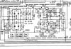
Both collector of Q9 and Q10 are 64V and -64V. sorry that my previous post is not clear about that. I did not measure the base of Q11 and I will do that tonight. but I guess my question is what is the purpose of Q11 in this circuit? I do not understand the circuitry between Q9 and Q10, with the Q11 and all the diode.
What are you reading on the collector of Q10 ? Do you have at least - .6 vdc on the base of Q11 ?

Nakdoc
nakamichi spoken here
A collector is not an input. The base is usually the "input", but here's the correct way to check transistors in circuit. Measure the voltage between base and emitter. For silicon transistors it is typically 0.6 volts. In many circuits, it can be less, but if it is more, the polarity of the voltage is important. With red on the base, greater than positive 0.7 volts on an NPN transistor = bad. Less than -0.7 volts = bad for PNP. Next measure collector to emitter voltage. Typically they will be different. If they are the same, or if base emitter voltages are the same, turn the amplicer power off, and switch the meter to resistance. Base emitter ought to read about 0.6 in diode test range. Collector to emitter ought to be infinite.
In your Accuphase, D9 and D10 zeners have to be ok, and Q9 emitter has to be 40 volts. Q11 samples this 40v and must have -0.6 on its base. Q11 collector has to be -39.4 volts. From your measurements Q9 is fine. Check Q11 for 0.6 volts base to emitter. If ok, then Q10 base to emitter must be very much less than -1 volt.
In your Accuphase, D9 and D10 zeners have to be ok, and Q9 emitter has to be 40 volts. Q11 samples this 40v and must have -0.6 on its base. Q11 collector has to be -39.4 volts. From your measurements Q9 is fine. Check Q11 for 0.6 volts base to emitter. If ok, then Q10 base to emitter must be very much less than -1 volt.
well, as you see from the diagram, Q9 and Q10 are regulator that provide output voltage of 40V and -40V for the pre-amp circuit. the output voltage is control by "Base" input of Q9 and Q10. and the "Base" input of Q9 and Q10 are completely different. I guess my real question is why is the "Base" input for Q9 is different from Q10? what is the purpose of Q11 in this case? Why is the "Base" input in Q9 is control by D9 and D10 but accuphase did not do the same for "Base" input of Q10 but instead use Q11? I am just trying to understand the circuit better.
A collector is not an input. The base is usually the "input", but here's the correct way to check transistors in circuit. Measure the voltage between base and emitter. For silicon transistors it is typically 0.6 volts. In many circuits, it can be less, but if it is more, the polarity of the voltage is important. With red on the base, greater than positive 0.7 volts on an NPN transistor = bad. Less than -0.7 volts = bad for PNP. Next measure collector to emitter voltage. Typically they will be different. If they are the same, or if base emitter voltages are the same, turn the amplicer power off, and switch the meter to resistance. Base emitter ought to read about 0.6 in diode test range. Collector to emitter ought to be infinite.
In your Accuphase, D9 and D10 zeners have to be ok, and Q9 emitter has to be 40 volts. Q11 samples this 40v and must have -0.6 on its base. Q11 collector has to be -39.4 volts. From your measurements Q9 is fine. Check Q11 for 0.6 volts base to emitter. If ok, then Q10 base to emitter must be very much less than -1 volt.
In your Accuphase, D9 and D10 zeners have to be ok, and Q9 emitter has to be 40 volts. Q11 samples this 40v and must have -0.6 on its base. Q11 collector has to be -39.4 volts. From your measurements Q9 is fine. Check Q11 for 0.6 volts base to emitter. If ok, then Q10 base to emitter must be very much less than -1 volt.
Is it possible that there is a small error in this schema? There is no way Q11 can sample the +40V... as long as there is really a connection between R35, D13 and ground (the dot between D13 and R35). Additionally, the +40V output is shortend to the ground via D13... I think the dot on the ground line is wrong.
Martin
I guess my real question is why is the "Base" input for Q9 is different from Q10? what is the purpose of Q11 in this case? Why is the "Base" input in Q9 is control by D9 and D10 but accuphase did not do the same for "Base" input of Q10 but instead use Q11? I am just trying to understand the circuit better.
Just remove the dot between R35 and D13. Prentend that you have -40V at the lower end of R36. Then you have a 1:1 voltage divider between R35 and R36 (both 33k). The point between R35 and R36 is halfway between +40 and -40V... at 0V. Add one diode to this in favour of R35, and you'll get about one diode voltage or -0.6V at the base of Q11.
If your negative voltage at the output is larger (= more negative) than this, the voltage at the base of Q11 will get more negative. This means that the current going through it is rising (being a PNP transistor), pulling the base of Q10 to a less negative voltage. The voltage at the emitter of Q10 follows its base, so the output voltage at the -40V output rises until it is again symmetric to the +40V, just as intended. It works the other way round, too. The caps C18, C20 and C24 dampen the whole thing against too fast reactions, supressing oscillations.
Martin
I just check the Q11 base voltage and I got 0.6mV, again, it is mV. so it is just like 0V. But I measure the resistor value of R35 and R36, they look ok. any idea?
A collector is not an input. The base is usually the "input", but here's the correct way to check transistors in circuit. Measure the voltage between base and emitter. For silicon transistors it is typically 0.6 volts. In many circuits, it can be less, but if it is more, the polarity of the voltage is important. With red on the base, greater than positive 0.7 volts on an NPN transistor = bad. Less than -0.7 volts = bad for PNP. Next measure collector to emitter voltage. Typically they will be different. If they are the same, or if base emitter voltages are the same, turn the amplicer power off, and switch the meter to resistance. Base emitter ought to read about 0.6 in diode test range. Collector to emitter ought to be infinite.
In your Accuphase, D9 and D10 zeners have to be ok, and Q9 emitter has to be 40 volts. Q11 samples this 40v and must have -0.6 on its base. Q11 collector has to be -39.4 volts. From your measurements Q9 is fine. Check Q11 for 0.6 volts base to emitter. If ok, then Q10 base to emitter must be very much less than -1 volt.
OK, I remove Q11 and finally comfirm that Q11 is bad, setting my DMM to diode test and testing emitter and base, I get almost 0V, switching the pole on my meter and check emitter and base again, I have 0V. so, it needs to replace. I wish I did it more carefully last time. What will be a good substitution for this transistor? according to my service manual, it is 2SA776. Any recommendation? Thanks a lot
I just check the Q11 base voltage and I got 0.6mV, again, it is mV. so it is just like 0V. But I measure the resistor value of R35 and R36, they look ok. any idea?
you are right, there is no connection from collector of Q11 to R35 D13, I just check the circuit broad to confirm that. now it make sense.
Is it possible that there is a small error in this schema? There is no way Q11 can sample the +40V... as long as there is really a connection between R35, D13 and ground (the dot between D13 and R35). Additionally, the +40V output is shortend to the ground via D13... I think the dot on the ground line is wrong.
Martin