N3w2Electron
New Member
Trying to wrap up a refurb of an SX-890 and can't get one channel to bias (DC Balance) and it won't get out of protection. At one point it would get out of protection but wasn't stable on on either channel when trying to DC Balance
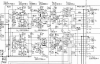
At this point, on the Right Channel I get ~ -35V at pin 12 and no response at all when changing VR6. I can set the Left Channel to zero. I can trace that negative voltage through Q7 to the base of Q20. I know that the Q20, Q7, and Q8 set is good because I swapped the Left Channel Q19, Q5, and Q6 ones into the Right Side and vice versa. They are original 2SC1775, 2SA979, and 2SC2291 configurations. The problem stayed on the Right channel regardless of which set of transistors was used. I've checked resistor values for everything touching that set and they all checked out.
I've read most of the SX-880 posts about protection issues. I've got the C418 oriented correctly. Seems like most of the other things noted don't seem to be the issue, but I haven't seen anyone mention this symptom.
I'd appreciate a tip for where to look for a most likely cause.
Thanks,
Craig
At this point, on the Right Channel I get ~ -35V at pin 12 and no response at all when changing VR6. I can set the Left Channel to zero. I can trace that negative voltage through Q7 to the base of Q20. I know that the Q20, Q7, and Q8 set is good because I swapped the Left Channel Q19, Q5, and Q6 ones into the Right Side and vice versa. They are original 2SC1775, 2SA979, and 2SC2291 configurations. The problem stayed on the Right channel regardless of which set of transistors was used. I've checked resistor values for everything touching that set and they all checked out.
I've read most of the SX-880 posts about protection issues. I've got the C418 oriented correctly. Seems like most of the other things noted don't seem to be the issue, but I haven't seen anyone mention this symptom.
I'd appreciate a tip for where to look for a most likely cause.
Thanks,
Craig