• The move to the new server is done. There are some software and database maintenance updates in process. This has us passing the hat around to help out. We appreciate any donations. Seriously, even a dollar helps. The payment page may be found here - https://www.audiokarma.org/support.html

Use for SV04 in cascodes VAS from Sansui AU-D11 II

GrisPato

Super Member
@Overundr1 brought to my attention the use of these components.
The middle line of Sansui amplifiers from this time, AU-D22/33/55X/G33/55X up to the X501 use a MVI03 in the cascoded VAS.
As far as my knowledge goes this is needed for the base- emitter biasing from the second transistor.
I would also be interested why it's that they use PNP on the positive rail and NPN on the negative. Is this because voltage gets inverted?
Really interested in some answers.
 
Register to hide this ad
@GrisPato - the simple version of answer would be "this is how cascoding works". The scope is to keep Vce constant for the active devices - which are Q5 and Q9.
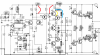
Blue line is a ideally constant voltage, in this case kept so by that multi-diode MV-103 (or SV-04 for AU-D11-II).
Vbe of the cascoding transistor, aka Q6 and Q8 is also pretty much constant, so you obtain the difference between two constant voltages - the yellow line (= Vdiode -Vbe) - which is maintained on the active devices.
Why a PNP on the (+) rail and a NPN on the (-) rail - because of the biasing and referencing the voltages to the V rails. The red line is the biasing voltage developed from the second LTP - the same voltage is applied on the VAS on active devices + R22 / R24. This is also what is setting the idle current in the VAS stage.
Hope this helps.

au-x501.PNG

Regards
 
Thanks @fojica for helping us out.
I think I understand what you mean but not sure yet.
Blue line is a ideally constant voltage, in this case kept so by that multi-diode MV-103
I assume that you mean with "constant" small variation in value?
Why do you need the diode string for that, or better said how does the diode string keep the voltage more constant?

referencing the voltages to the V rails.

This I am not sure about. You want a higher voltage at the emitter then the collector for voltage gain?
I can see in other designs that the VAS also when it's in class A has the emitter to positive rail.
If you have time I would love if you can explain a little more.
 
I guess what bothers me about using those multi string diodes is the accuracy of using a thermally sensitive device to maintain a desired constant voltage even with a low current application. SV04's will vary between 2.1 and 2.4v depending on temperature, a rather large voltage swing. Would not a ccs circuit be a better solution?
 
You want a higher voltage at the emitter then the collector for voltage gain?
Not necessarily, the potential or the voltage of the rail is only limiting voltage excursion of VAS stage and further...pre-drivers, drivers, outputs....in other words, it will dictate your maximal output power in the end. Think about P = (V*V)/R , which R in this case is the impedance of the load (speaker).
What matters here is that the voltage developed on R13 = Vbe of Q5 (VAS) + VR22 =~ 0.65V + VR22. It's obvious that changes in VR13 will lead to changes in VR22, even if Vbe of Q5 will also increase slightly once that current through R22 is increasing (caused by increased current in R13). Similarly, a decrease in current through R13 leads to a lesser current in R22 and a slightly less Vbe (but we are talking of mV here anyway, depending on the Q5 beta of Hfe).
In general, you must also take into account the power dissipated in the VAS transistor - once increasing the dissipation, Vbe will get lower. But here, since we are talking about cascoded VAS, there is no big change in power dissipation (this is also an "indirect" goal of the cascode).
You can take an arbitrary example....assume 1mA the current through R13...and calculate the VAS current (the one passing through R22). And then change the initial value of 1mA, up/down +/- 0.2mA....see where you get :)

Would not a ccs circuit be a better solution?
SV04 voltage will vary of course with current, but the current variation is anyway small to cause serious voltage variations. Temperature should not be a big concern here, as they are not placed near the heatsink to be affected....and anyway, if they are (and should be) close to the VAS device and the cascoding device, then temperature variation would be more or less the same in all elements involved - so no big change due to temperature. This is how I see it.
But, if you were thinking to replace kR35 for example (AU-D11-II sch) with a CCS, then yes, that would be an improvement because cascode voltage imposed by the SV04 will be more stiff related to voltage rail ripple. :thumbsup:
In case you have such a multi-diode placed on output or driver transistors heatsink, then that's a different story because we are speaking of thermal feedback in that case (increasing temperature will lover the voltage in the multi-diode, which for this particular scenario is usually connected somewhere in input stage to adjust the bias tracking the heatsink temperature - STV diodes were used sometimes like this if I'm not wrong).

Hope I answered your questions.
Regards

 
I assume that you mean with "constant" small variation in value?
Why do you need the diode string for that, or better said how does the diode string keep the voltage more constant?
Check attached graph....it's taken from some other thread here on the forum.
For a specific current passed, you have a resultant voltage developed....after all, they are similar with 3 x 1N14148 or 4 x 1N4148, like in the graph. It's the normal PN silicon junction variation with current.
And what I answered above - if you replace R35 with a CCS, then you'll get a stiffer voltage on the MV-103 / SV-04.
Vce of Q5 (VAS) = Vdiode - Vbe of Q6 = Vdiode - ~0.65. It won't be 100% constant, obviously, but the lesser the variation, the better.

"Why do you need the diode string for that" - you don't, actually, you can use LED's for example....anything that develops a "pretty constant" voltage over it.
It's clear now ? :D
 
Last edited:
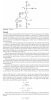
Here is the cascode explained - probably better than I did. In the attached example the circuit is referenced to GND....in the case that you asked for, reference is V+ rail instead of GND. To be more exact, the cascode is referenced to the emitter of Q5 VAS. Otherwise the same principle applies.
That +2V bias for the cascoding transistor can be "anything" that develops constantly about 2V - like a 2V source or battery, diodes string, LED.
cascode_explained.jpg

P.S. CE = common emitter
 
@Overundr1 - you're welcome, glad that it helped :thumbsup:

@GrisPato - related to your question "Why do you need the diode string for that" - you can have a look on AU-D11 (non-II) schematic, there those string diodes were not used, instead they used a "fixed Vbe multiplier" in their place.
Also is worth to look on the red line on that schematic, which is the signal flow - maybe it will help you to understand better the referencing to the rail voltages instead of referencing to ground (GND), how currents flow and how voltages are developed.
Keep in mind that voltage is just the potential difference between two points in the circuit....and none of those points is mandatory to be GND or connected somehow to GND. Maybe this explains it better (I hope so). :)
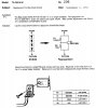
Below attachment (found also here on the forum -> https://audiokarma.org/forums/index.php?threads/odd-diode-in-sony-str-v3.754656/) is a recommendation from a Sony bulletin. Probably involves also some thermal feedback in their case as it looks to be mounted on the heatsink, but the electrical circuit in itself is identical with the substitution done in AU-D11 and works in the same way.

sv04s replacement by Sony.jpg

Regards
 
Ok, interesting but I have to admit, the details are to advanced for my really basic knowledge. So I will study the pointers you gave.
Can I come to the simple conclusion that the diodestring was/ is adequate for the job at hand. Probably a balance between space, component cost and accuracy.
 
Can I come to the simple conclusion that the diodestring was/ is adequate for the job at hand. Probably a balance between space, component cost and accuracy.
You can see it that way.
From my perspective, I would say it's a "predictable way to drive the DD block from the LTP input stage". Obviously, with the diodes string it's not a linear correspondence between current in the LTP and voltage developed to drive the DD block. This is easily seen in the graph posted sometime previously.
BUT, and this is the interesting thing...if you look at the B-2105 MOS Vintage schematic, then you'll see there 1K resistors in LTP drains instead of MV-103 or similar diodes string :) Now with 1K we have a linear correspondence...but also much different than the one with diodes string. Which version is better and why they put 1K resistors there unlike before....well, I don't have an answer to this. It's still a mystery for me. :idea: Maybe I'll try with 1K resistors at some point, just for curiosity :D
What I've written above covers only the diodes string used in the input stage, on double JFET drains.
For the SV-04 on VAS cascodes, let's say they are a "constant and low noisy enough" voltage source to bias the cascode transistors (Q6 and Q8 for AU-X501).

Regards,
Tibi
 
Last edited:
Back
Top Bottom