• The move to the new server is done. There are some software and database maintenance updates in process. This has us passing the hat around to help out. We appreciate any donations. Seriously, even a dollar helps. The payment page may be found here - https://www.audiokarma.org/support.html

Yamaha B-2 - Unstable bias and very tight adjustment range

david winter

Classical music lover.
Hi,

I'm trying to figure out what can cause the -85V supply to drop to -60V when the bias increases up to around 40mV.
With no bias, I get the +85V and -85V voltages correct.
Adjusting the bias on either channel makes the -85V drop down to -60V.
I checked the transistors on the negative rail and didn't find anything wrong. I only replaced a 2SA872 with insufficient gain and a 2SC1439 with too high gain (could be ok but I preferred replacing it).

I'm not going into overhauls, but so far I did the following:
- Electrolytics replaced (including the big ones on the psu)
- Replaced all 2SC458/2SC1345
- Replaced both protection relays

On the power output boards, I replaced:
- All fuse resistors by non-flamable ones with correct wattage
- The four 0.1µF
- All 2SA810 (TR107, TR108, TR109, TR122, TR124) by TTA-004
- All 2SC1452 (TR110, TR121, TR123) by TTC-004
- Bias trimmers by multi-turn ones

Diodes D101, D102, D110, D111 test fine at 1.36V-1.4V

The input N-FET (TR104, TR105) test very close, so I don't think they are causing any trouble.
Vgs-off: -0.44V @ Id=5.1µA / -0.46V @ Id=4.6µA
Vgs-in @ Id=5.00µA: 0.18V / 0.19V
gfs @ Id=3.0mA to 5.0mA: 14.9mA/V / 14.2mA/V
Idss = 2.43mA at Vds=2.99V / 3.01V
Rds-on @ Id=5.0mA: 50.1R / 55.4R

Any help welcome :)
 
Last edited:
Register to hide this ad
What do you mean more precisely ?
I tested them individually before installing, which allowed matching TR107/TR108 and the gains for the complementaty drivers.
I checked their placement twice. No mistake there unless TTA-004 and TTC-004 aren't suitable replacements.
 
Id put the originals back in vs the TT's and see how it behaves .

Hopefully the V-fets are ok .

Nashou
 
What do you mean more precisely ?
I tested them individually before installing, which allowed matching TR107/TR108 and the gains for the complementary drivers.
I checked their placement twice. No mistake there unless TTA-004 and TTC-004 aren't suitable replacements.
What you are describing resembles a condition where the auto-bias kicked in. It could be something else but that is what I would scrutinize first.

1) look at all wire connections for the +/-85v supply to the driver boards. Scrutinize your +/- 85v supply parts you replaced. on the main PSU PCB. -> in case your 85v supply is unstable or collapses under load, then the autobias kicks in.

2) On the driver boards, Investigate your auto-bias circuit and particularly the orientation of those diodes. Read the service manual section on the autobias.

then I would look at the replacement transistor choices

3) On the driver boards, the TTA/TTC should work on the unity gain section but there are better replacements. For the VAS, ( TR #107 & #108, IIRC) TTA004' Cob is even more relevant than in the buffer section, and with TTA the Cob is higher than the originals (17pf vs 3pf) and would not work as well as a KSA1381/2SA1380. The potential of TTA004 higher Cob causing oscillation is a general concern but not likley the case here.
4) What did you replace the rest of the transistors with?
5) What is your DC Bal when this happens?
 
Last edited:
Sorry for late reply, I was busy on with some other gear.
I only replaced the transistors mentioned above. All others and all diodes were left in place.
The problem doesn't seem to be related to the TTA/TTC. One channel adjusts fine at 40mV.

The other driver board has a problem. Its bias trimmer isn't yet replaced by a multiturn, but has been checked and works.
What happens is that the bias stays at around 20mV and will then very rapidly jump. The DC balance is at 10V (!) and won't adjust.
I'll try to understand what's wrong with this board.

Edit:
I have checked all diodes which test ok under 5mA.
All original transistors test ok, except the bias one (T117) which gain is off-spec. Not sure how much this can affect the bias circuit, but I'll test with a replacement just in case.

TypeHfe @ 5mAHfe from specsVbe @ 5mA
T1012SA872344250min0,77
T1022SC1775603160min0,76
T1032SC1775536160min0,76
T1062SC1439160150 typ.0,74
T1112SA872409250min0,77
T1122SC7348940min0,71
T1132SA5619140/4000,74
T1142SC1775607160min0,76
T1152SC1775622160min0,76
T1162SA872343250min0,77
T1172SA858109150 typ.0,75
T1182SC1439154150 typ.0,74
T1192SC1775586160min0,76
T1202SA872343250min0,77
 
Last edited:
The DC balance is at 10V (!) and won't adjust.
That is a critical factor - When you have that high of DC at the output, your DC protect kicked in and you will not be able to adjust bias.

Next steps:
0: you should probably replace both DC and Bias trim-pots to rule them out.
1: For DC to be that high, you likely lost ground to the front-end section of that amp board or one of the input diff pair jfets is dead. My money is on the lost ground to the front end.
2: If above not the case, revisit your replacements, with focus on the NFB components, and check for any bad solder joints. No need to focus on parts gain here. Focus on pin-out orientation, solder joints, shorts.


edit:
If none of the above works, I can point you to an experienced tech in France.
 
Last edited:
Trimmers were replaced, which didn't change anything (I tested them sometime ago and didn't notice anything wrong).
Here's what I get:
Driver 1: bias stays at 4mV, 37V output, whether I put it on the left or right place.
Driver 2: bias adjusts to 40mV, 19V outputn, whether I put it on the left or right place.
I'm not sure about those replacement transistors, and don't want to put originals back which are known to fail.
I'd rather ask you what to put in place of those TTA/TTC.
 
What is your DC offset?
Stop focusing on the bias until you get the DC below 2v or so, preferably within few mV.
You will not be able to do anything with the bias when the DC is high and the unit is in protection.

Did you check your front end ground?
Take a wire and solder one end at the ground solder joint of your signal IN ground and the other end at the center ground of the power supply.
Then test your DC. See if you can adjust it

It is not the transistors you used either ….unless you do not have the correct orientation
Start posting photos with good resolution, front and back of the driver board with issues
 
Last edited:
I swap the boards with the unit turned off, AND after having discharged all power supplies.
If I want to test with only one driver in place, I disconnect the rails on the other vfet board and discharge as well.
 
I swap the boards with the unit turned off, AND after having discharged all power supplies.
If I want to test with only one driver in place, I disconnect the rails on the other vfet board and discharge as well.
Yes but you are working with faulty boards and vfets inside the same unit. There is a high probability something will go very wrong with this approach.
The driver boards should be solid before putting the vfets back in the unit. That is my approach, but in the end the unit is yours, so your decision.

Go through the above recommendations about DC offset and also post some hi res photos of the front and back on the faulty board. I still believe that the first next step is to ensure you have ground to your front-end by using a wire between our signal IN ground and PSU center ground, then check DC offset.
This can be done with the vfets outside the units and nothing else. No need to continue to worry about the ability to adjust bias when you have such high DC offset which puts your amp in protection mode.
 
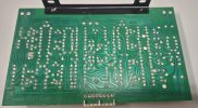
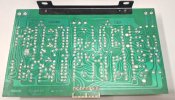
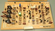
I uploaded some pictures of the driver boards and removed the transistors for testing.

Edit: I checked the voltages at the header going to the (empty) FET boards. Both +85V and -85V supplies are good while testing.
One driver board (the second one shown below, without the heatsinks on the TTA/TTC transistors) has a problem:
PS = -10.7V (0V on the other)
NF = -21.7V (0V on the other)
NS = -21.4V (-1.1V on the other)

The table below shows the FET tests.
The first column is my own marking to put them back at the right place.
What are the handwritten values in red and black between the pins ?

Vgs(off) @ Id=5µAVgs(on) @ Id=5mAgfs @ Id = 3 to 5mARds(on) @ Id=5mA and Vgs=0V
A1 (2SJ26)-7.25 V-5.31 V23.3 mA/V< 1.0 Ω
A2 (2SK76)-6.69 V-4.84 V20.5 mA/V< 1.0 Ω
A3 (2SJ26)-6.73 V-5.32 V24.3 mA/V1.5 Ω
A4 (2SK76)-6.63 V-4.84 V22.4 mA/V< 1.0 Ω
B1 (2SJ26)-6.70 V-5.17 V24.4 mA/V1.3 Ω
B2 (2SK76)-6.92 V-4.99 V16.1 mA/V< 1.0 Ω
B3 (2SJ26)-6.64 V-5.16 V25.0 mA/V1.5 Ω
B4 (2SK76)-6.51 V-4.76 V20.7 mA/V< 1.0 Ω


20260601_150835.jpg

20260601_150830.jpg

20260601_150438.jpg

20260601_150441.jpg
 
Last edited:
I uploaded some pictures of the driver boards and removed the transistors for testing.

Edit: I checked the voltages at the header going to the (empty) FET boards. Both +85V and -85V supplies are good while testing.
One driver board (the second one shown below, without the heatsinks on the TTA/TTC transistors) has a problem:
PS = -10.7V (0V on the other)
NF = -21.7V (0V on the other)
NS = -21.4V (-1.1V on the other)

The table below shows the FET tests.
The first column is my own marking to put them back at the right place.
What are the handwritten values in red and black between the pins ?

Vgs(off) @ Id=5µAVgs(on) @ Id=5mAgfs @ Id = 3 to 5mARds(on) @ Id=5mA and Vgs=0V
A1 (2SJ26)-7.25 V-5.31 V23.3 mA/V< 1.0 Ω
A2 (2SK76)-6.69 V-4.84 V20.5 mA/V< 1.0 Ω
A3 (2SJ26)-6.73 V-5.32 V24.3 mA/V1.5 Ω
A4 (2SK76)-6.63 V-4.84 V22.4 mA/V< 1.0 Ω
B1 (2SJ26)-6.70 V-5.17 V24.4 mA/V1.3 Ω
B2 (2SK76)-6.92 V-4.99 V16.1 mA/V< 1.0 Ω
B3 (2SJ26)-6.64 V-5.16 V25.0 mA/V1.5 Ω
B4 (2SK76)-6.51 V-4.76 V20.7 mA/V< 1.0 Ω


View attachment 3774026

View attachment 3774027

View attachment 3774028

View attachment 3774029
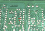
1) difficult to tell if you have shorted solder joints from the low res photos. Use a magnifying glass and look over the entire back of the PCB. I am sure this is just low res, but as an example, the solder joint looks shorted to the trace next to it, on the photo you shared.
1780342955997.png


2) Question about Q10: Take a closeup photo of Q10 so I can see where the pins go.


3) The readings you took using the Atlas Pro have little value or relevance. The markings on the back of the transistors were take by Yamaha, at parameters representative of the working conditions of the transistors in circuit, read: real wold conditions, much higher on the IV region than the Atlas Pro can deliver. That said, it is difficult to know what exact parameters they tested for.

For instance I test at idle conditions for directional matching but also look at the rest of the IV spectrum using a high power curve tracer. I mark the transistors I test with Vgs value at idle Ids and voltage rails for Vds. No need to stress on rds(on) matching because the transconductance / "gain" is directly proportional with the rds(on). Read: if you match in Vgs, you are also indirectly matching on rds(on).

The above is a high level description. For precise matching, temperature coefficient needs to also be taken into account since the vfets have a negative temp coefficient, as in, hey need to reach operating temperature for the Ids to settle since the hotter the transistor, the lower the Ids. This is a wonderful characteristic of vfets. There is more to this, but the above should be enough to speak to your vfet testing call out.

In summary: count your blessings that the vfets are Okay. Do not re-introduce them until you get solid driver boards.
 
Maybe it’s just the low-res photos but I can’t see the third leg of the bias trimmer on the solder side of the board. Looks like it’s not soldered in. See below:

41468A67-1E6A-43A5-A6FD-6F63D40775D0.jpeg
 
not needed, free standing, but for mechanical reasons it should still be soldered. I suspect that once the pots are replaced, he will solder the third leg
It helps to look at the schematic once in a while. The two trimmer legs are clearly tied together. Oh well …
 
I saw that too but assumed he left it soldered so he does not have to de solder another leg if he did not have to.
That empty hole just grabbed my attention and I always expect to see three soldered legs on a trimmer. I also often see that bias trimmer with two legs tied together but somehow 2 + 2 = 3. :-)
 
Back
Top Bottom