• The move to the new server is done. There are some software and database maintenance updates in process. This has us passing the hat around to help out. We appreciate any donations. Seriously, even a dollar helps. The payment page may be found here - https://www.audiokarma.org/support.html

Yamaha RX-V685 Entering Protect Mode: Need Troubleshooting Help

Levy4u

New Member
Hello everyone,

I've run into an issue with my Yamaha RX-V685 receiver. It's about 3 years old and has recently entered protect mode with the error "DC PRT: 255". When I turn it on, it shuts off within about 3 seconds. I'm comfortable with electronics, have a multimeter, esr tester, just have never messed with a receiver.

Here's what I've done so far:
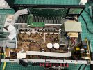
  1. The unit has always been in a filtered, active ventilated, rack and used for streaming movies.
  2. Disconnected all speakers and found that the surround back (zone 2) has a 57v present.
  3. Checked the speaker terminals: No issues noticed.
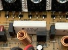
  4. Opened the unit. I preemptively cut the output transistors for sbL and sbR (having heard they're common culprits for this error). Unfortunately, the issue persists.
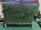
  5. No bulging capacitors, visible damage, or hot spots. Traces seem intact.
  6. Checked noble resistors for each channel: Starts at 0, goes to 1.1 but settle around 0.6ohm.
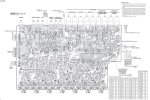
  7. I have the service manual, but I'm struggling to follow the board routes and determine which parts might be causing the issue.
Questions:
  • Can I test the components while they're still soldered to the board (with no power, of course)? Or do they need to be removed?
  • Any pointers on which parts might be causing this error or how to troubleshoot further would be greatly appreciated.
I will recheck anything needed to make sure I'm covering all the bases. Thank you in advance for any guidance!


IMG_3006.jpeg
 

Attachments

  • 2023-10-08_18-26-06.jpg
    2023-10-08_18-26-06.jpg
    145.3 KB · Views: 13
  • IMG_3005.jpeg
    IMG_3005.jpeg
    105 KB · Views: 15
  • IMG_3016.jpeg
    IMG_3016.jpeg
    201 KB · Views: 11
Last edited:
Register to hide this ad
Disconnected all speakers and found that the surround back (zone 2) has a 57v present.
Assumed you measured this at the emitter resistors, ideally the middle pin.

57V is near rails voltage, the common fault scenarios are output or driver transistor (eg, Q1036) c-e short. Service manual has rail at 61V so there is some IxR and Vbe volt drop, Suggest test the driver transistors, try incircuit since looking for a c-e short.
 
Assumed you measured this at the emitter resistors, ideally the middle pin.

57V is near rails voltage, the common fault scenarios are output or driver transistor (eg, Q1036) c-e short. Service manual has rail at 61V so there is some IxR and Vbe volt drop, Suggest test the driver transistors, try incircuit since looking for a c-e short.
I checked the output voltage initially by probing the terminals with the unit completely together. Once I opened it up, i cut the output transistors, tested it again after resetting, and when it still was shutting off, I took it all apart.

Using my DMM in diode mode, I check all the driver transistors (Q1036, C004B NPN type):

B-E .6
B-C .6
E-B 0L
E-B (SBL) .9 rises to 0L
C-B 0L
C-B (SBL) .9 rises to 0L
C-E 0L
C-E (SBL) .8 rises to 0L
E-C (SBR) 0L
E-C (SBL) .8 rises to 0L
E-C (all others) .49 stable

Not sure if these are expected or if switching positive and negative on the DMM would charge the components in between reads.


I also checked the A004B PNP (Q1043) types, all channels matched:

B-E 0L
B-C 0L
E-B .6
C-B .6
C-E .488 stable
 
Last edited:
Graphic below from markthefixer explains in a nutshell how to diode test transistors and expected results.

I checked the output voltage initially by probing the terminals with the unit completely together.
Not clear what terminals, speaker terminals or transistor terminals/legs or...

i cut the output transistors,
I assume you did not cut the transistor legs!


I don't see the expected c-e short, the next step would have been to take some voltage measurements...
 

Attachments

  • DiodeTest.JPG
    DiodeTest.JPG
    42.8 KB · Views: 16
Not clear what terminals, speaker terminals or transistor terminals/legs or...
Speaker terminals, the +/- physically on the back of the receiver.

I assume you did not cut the transistor legs!
Yeahhh, I did the first thing I saw as a fix. Was not thinking too much.

I have replacement sets of output transistors on the way. I can solder them in and repeat testing if that would change any of the results.

I don't see the expected c-e short, the next step would have been to take some voltage measurements...
Voltage measurements of? Anything specific or just everything in the SBL and SBR circuit? I think I can follow it a bit better now after a bunch of reading.

And is this with no power or do I need to put it back together and power it up?
 
Speaker terminals, the +/- physically on the back of the receiver.
I'm surprised you saw 57V at the spkr terminals. The amp should be in protection so the speaker relays should not be activated, ie, no connection to the amp. Under such cases the large white emitter resistors (in front of the output transistors) is a good measurement point, prefer the middle leg.

or do I need to put it back together and power it up?
Since you've disassembled the unit, best to have a look around.
The more likely candidates are Q1036, 1050. Q1015 should also be checked.
Recheck these transistors using the graphic above.
 
I'm surprised you saw 57V at the spkr terminals. The amp should be in protection so the speaker relays should not be activated, ie, no connection to the amp. Under such cases the large white emitter resistors (in front of the output transistors) is a good measurement point, prefer the middle leg.


Since you've disassembled the unit, best to have a look around.
The more likely candidates are Q1036, 1050. Q1015 should also be checked.
Recheck these transistors using the graphic above.

I bypassed protection via pushing info + tone control I believe.

Q1036 (and same transistors for the other channels) was measured, post #3 are the values for them. SBL noted would be 1036, SBR is 1037, "all others" are referencing that transistor location for all other channels. Same goes for Q1043 1044, "all others".

To make sure I'm not overlooking something, the diagram I found for A004B and C004B show the collector in the middle. This is how I measured previously. Is this wrong as it appears the Base is the middle dot in the other diagram you posted?
ttc004b-pinout.jpg
tta004b-pinout.jpg

2023-10-09_17-51-56.jpg

I did not check 1015 yet.

1050A/C and 1051A/C were the ones I cut.
 
Last edited:
To make sure I'm not overlooking something, the diagram I found for A004B and C004B show the collector in the middle. This is how I measured previously. Is this wrong as it appears the Base is the middle dot in the other diagram you posted?
These transistors are ecb, always refer to datasheets for pinout, ie, google TTC004B datasheet.
The "markthefixer" graphic is a generic representation covering all BJT's regardless of pinout.
 
Back
Top Bottom