smurfer77
Super Member
Well the funny thing about me writing this thread is that I don't even own an amp that uses the 2SK97. I got interested in the topic because I was doing some measurements of the 2SK129A (another dual N-JFET) which appears in my Sansui AU-X11. Anyway, it looks like the 2SK97 is used in some Sansui, Sony and other units, but specs are unconfirmed and subs therefore not certain.
There are some specs over on a Stereonet thread, reposted from here, which seems to be by far the most detailed account of the 2SK97 specs. In fact, it looks like it was from a spec sheet. But nobody can find the spec sheet to confirm, and also those FET spec ranges are always big and it would be good to know typical values for choosing a sub.
From those threads we have:
2SK97 dual N-Channel Junction FET
in dual in line case.
Pins:
1 : Drain 2
2 : Gate 2
3 : Source 2
4 : Source 1
5 : Gate 1
6 : Drain 1
Absolute Maximum Ratings:
Vdgo = 30 V
Vsgo = 30 V
Id = 20 mA (1 FET)
Ig = 5 mA ( 1 FET)
Ptot = 210 mW (2 FETs)
Channel Temp. 100 grdC.
Storage Temp.: -50 to 120 grdC.
Characteristics:
Idss at Vds=10V, Igs=0 : min 0.9 mA, max 14.3 mA
Pinch off Voltage at Vds=10V, Id=30uA : min 0.18V, max 1.49 V
Forward Transfer Conductance at Vgs=0V, Vds=10V : min 6.3 mS
Reverse Transfer Capacitance (same conds.): typ 2.4 pF
Input noise voltage at Rg=10kOhm, f=1kHz:
typ 13 nV / sqareroot Hz
Vgs difference between 2 FETs at Id=1mA: max 70 mV
Classification:
Rank 1 : Idss = 0.9 to 5.5 mA
Rank 2 : Idss = 4.5 to 9.9 mA
Rank 3 : Idss = 8.1 to 14.3 mA
@Ronito6 sent me a 2SK97 to measure and here. It is marked "KC22" and I guess one of those numbers might refer to "rank 2" Idss. Ronito could confirm for us which amp this device came from for reference.
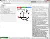
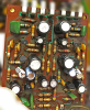
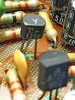
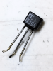
Ok, so first thing I did was confirm the pin-out. It does actually follow the pin-out noted in the specs posted above. In the pic here I probably have the chip upside down, but it doesn't matter - see the white bar printed on the chip, that is the end with the drains; gates are in the middle, and sources are on the other end. The unit passed quick diode check too. So I hooked up two DC supplies and off we went with some measurements.

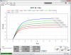
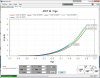
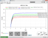
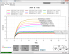
I ran through with Vgs = 0 V and Vds = 10 V on both FETs and got very similar results, so the data below is only for one of the FETs, not both. There are a couple of weird 'kinks' in the data, which appeared for both FETs.

You might notice one apparently weird Vds choice of 13.3V. I put that in because a quick glance at the Sansui AU-717 manual shows about 13.3V across drain and source. Also you can see from the measured data that Idss is just over 8mA.

Note that at Vds 15V and above the temperature of the device starts to shoot up as the current initially way higher than 8mA, then it heats up and the negative temp dependence brings the current back down over time. At 15V the device went up to 35 C and at 20V it went up to 50C and I didn't push it any further even though specs previously listed suggest 30V is possible. If your 2SK129 is heat sinked, you are going to get a bit different results to what I have here, as evidenced by the effect of putting my thumb on the device to bring it up/down to 37C. FYI, ambient when taking measurements was about 20C
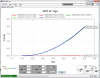
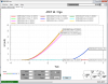
I took a few extra data points to get a smooth curve for current vs v_gs.


Below is the data for the above graphs, and you can see transconducance calculated and Vgs_off (= - V_pinch_off). Transconductance averages around 12, and you can see in the data and graph below it swings a lot depending on where you are operating - beware there is a bunch of uncertainty in those data points and higher level of uncertainty in the slope (since we have the errors from 4 data points for each value), so just take that as a rough guide. As a guide I would say the transconductance is in the 10-20 range typically.

I took some averages of the calculated V_gs_off from the usable part of the data (small values or current have large error) and get about -0.8V (i.e. V_p = 0.8V). V_p was 0.78 as measured by another technique (simply taking the voltage over gs without a Vgs voltage source (but with Vds in place) exploiting the internal large impedance of the DVM as a load). Let's just say V_p ~ 0.8V.
Summary:
- pins confirmed. Drains are next to the white bar printed on top (there is typical marking underneath too, which I would always check in case the top was printed on backwards).
1 : Drain 2
2 : Gate 2
3 : Source 2
4 : Source 1
5 : Gate 1
6 : Drain 1
- Also specs others have quoted mention 30V is okay, I wouldn't use this thing past 15V Vds.
- Matching between FETs was good enough it wasn't worth my showing both sets of data. But there was up to 10% difference. The 1%
- Idss from previous reports was said to be: Vds=10V, Igs=0 : min 0.9 mA, max 14.3 mA. I measured just over 8mA for both FETs. It seems likely that one of the "2"s in the "KC22" on my device do in fact indicate rank 2. Whether or my Idss is typical for rank 2 or hand-picked for this amp (Ronito6, it was a Sansui AU-717 this came from?) I couldn't say. So I think the classifications (Rank 1 : Idss = 0.9 to 5.5 mA; Rank 2 : Idss = 4.5 to 9.9 mA; Rank 3 : Idss = 8.1 to 14.3 mA) posted by others could also be pretty accurate.
- Pinch off voltage was previously quoted as (at Vds=10V, Id=30uA): min 0.18V, max 1.49 V. That is quite a large range. I measure about 0.8V for both FETs. (again, this could be well matched across the pair, but might not be typical if we measure other packages).
- Transconductance (at Vgs=0V, Vds=10V) was previously quoted as "min 6.3 mS". This is probably true too. I am calling the my device 10-20 mS transconductance - see graph, the max goes just over 20 mS.
So it looks to me like those specs quoted could be legit from a spec sheet originally, and we have filled in some gaps here, especially with regard to typical values.
In terms of a substitute, if you look over at another thread of mine you will find some number on currently available dual N-JFETs. In particular:
LSK389B: Idss ~7.8mA (Vds=10V,Vgs=0V), Gm ~ 21 (Vds=10V,Vgs=0V), Vp ~ 0.62 V (Vds=10v) It looks to be a good substitute. Make sure you get the "B" version/rank if your 2SK97 is rank 2. Rank 1 will likely be closer to the 389A and rank 3 could be either B or C version depending on the actualy Idss needed in your machine.
Keep in mind that FETs parameters vary from sample to sample, much more than BJTs. Matching within the monolithic pair will be good, but from package to package, it can get wild. I recommend ordering a few units, and measuring (or if you don't have that capability, at least you could swap out for another if it just doesn't sound quite right).
There are some specs over on a Stereonet thread, reposted from here, which seems to be by far the most detailed account of the 2SK97 specs. In fact, it looks like it was from a spec sheet. But nobody can find the spec sheet to confirm, and also those FET spec ranges are always big and it would be good to know typical values for choosing a sub.
From those threads we have:
2SK97 dual N-Channel Junction FET
in dual in line case.
Pins:
1 : Drain 2
2 : Gate 2
3 : Source 2
4 : Source 1
5 : Gate 1
6 : Drain 1
Absolute Maximum Ratings:
Vdgo = 30 V
Vsgo = 30 V
Id = 20 mA (1 FET)
Ig = 5 mA ( 1 FET)
Ptot = 210 mW (2 FETs)
Channel Temp. 100 grdC.
Storage Temp.: -50 to 120 grdC.
Characteristics:
Idss at Vds=10V, Igs=0 : min 0.9 mA, max 14.3 mA
Pinch off Voltage at Vds=10V, Id=30uA : min 0.18V, max 1.49 V
Forward Transfer Conductance at Vgs=0V, Vds=10V : min 6.3 mS
Reverse Transfer Capacitance (same conds.): typ 2.4 pF
Input noise voltage at Rg=10kOhm, f=1kHz:
typ 13 nV / sqareroot Hz
Vgs difference between 2 FETs at Id=1mA: max 70 mV
Classification:
Rank 1 : Idss = 0.9 to 5.5 mA
Rank 2 : Idss = 4.5 to 9.9 mA
Rank 3 : Idss = 8.1 to 14.3 mA
@Ronito6 sent me a 2SK97 to measure and here. It is marked "KC22" and I guess one of those numbers might refer to "rank 2" Idss. Ronito could confirm for us which amp this device came from for reference.
Ok, so first thing I did was confirm the pin-out. It does actually follow the pin-out noted in the specs posted above. In the pic here I probably have the chip upside down, but it doesn't matter - see the white bar printed on the chip, that is the end with the drains; gates are in the middle, and sources are on the other end. The unit passed quick diode check too. So I hooked up two DC supplies and off we went with some measurements.
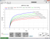
I ran through with Vgs = 0 V and Vds = 10 V on both FETs and got very similar results, so the data below is only for one of the FETs, not both. There are a couple of weird 'kinks' in the data, which appeared for both FETs.
You might notice one apparently weird Vds choice of 13.3V. I put that in because a quick glance at the Sansui AU-717 manual shows about 13.3V across drain and source. Also you can see from the measured data that Idss is just over 8mA.
Note that at Vds 15V and above the temperature of the device starts to shoot up as the current initially way higher than 8mA, then it heats up and the negative temp dependence brings the current back down over time. At 15V the device went up to 35 C and at 20V it went up to 50C and I didn't push it any further even though specs previously listed suggest 30V is possible. If your 2SK129 is heat sinked, you are going to get a bit different results to what I have here, as evidenced by the effect of putting my thumb on the device to bring it up/down to 37C. FYI, ambient when taking measurements was about 20C
I took a few extra data points to get a smooth curve for current vs v_gs.
Below is the data for the above graphs, and you can see transconducance calculated and Vgs_off (= - V_pinch_off). Transconductance averages around 12, and you can see in the data and graph below it swings a lot depending on where you are operating - beware there is a bunch of uncertainty in those data points and higher level of uncertainty in the slope (since we have the errors from 4 data points for each value), so just take that as a rough guide. As a guide I would say the transconductance is in the 10-20 range typically.
I took some averages of the calculated V_gs_off from the usable part of the data (small values or current have large error) and get about -0.8V (i.e. V_p = 0.8V). V_p was 0.78 as measured by another technique (simply taking the voltage over gs without a Vgs voltage source (but with Vds in place) exploiting the internal large impedance of the DVM as a load). Let's just say V_p ~ 0.8V.
Summary:
- pins confirmed. Drains are next to the white bar printed on top (there is typical marking underneath too, which I would always check in case the top was printed on backwards).
1 : Drain 2
2 : Gate 2
3 : Source 2
4 : Source 1
5 : Gate 1
6 : Drain 1
- Also specs others have quoted mention 30V is okay, I wouldn't use this thing past 15V Vds.
- Matching between FETs was good enough it wasn't worth my showing both sets of data. But there was up to 10% difference. The 1%
- Idss from previous reports was said to be: Vds=10V, Igs=0 : min 0.9 mA, max 14.3 mA. I measured just over 8mA for both FETs. It seems likely that one of the "2"s in the "KC22" on my device do in fact indicate rank 2. Whether or my Idss is typical for rank 2 or hand-picked for this amp (Ronito6, it was a Sansui AU-717 this came from?) I couldn't say. So I think the classifications (Rank 1 : Idss = 0.9 to 5.5 mA; Rank 2 : Idss = 4.5 to 9.9 mA; Rank 3 : Idss = 8.1 to 14.3 mA) posted by others could also be pretty accurate.
- Pinch off voltage was previously quoted as (at Vds=10V, Id=30uA): min 0.18V, max 1.49 V. That is quite a large range. I measure about 0.8V for both FETs. (again, this could be well matched across the pair, but might not be typical if we measure other packages).
- Transconductance (at Vgs=0V, Vds=10V) was previously quoted as "min 6.3 mS". This is probably true too. I am calling the my device 10-20 mS transconductance - see graph, the max goes just over 20 mS.
So it looks to me like those specs quoted could be legit from a spec sheet originally, and we have filled in some gaps here, especially with regard to typical values.
In terms of a substitute, if you look over at another thread of mine you will find some number on currently available dual N-JFETs. In particular:
LSK389B: Idss ~7.8mA (Vds=10V,Vgs=0V), Gm ~ 21 (Vds=10V,Vgs=0V), Vp ~ 0.62 V (Vds=10v) It looks to be a good substitute. Make sure you get the "B" version/rank if your 2SK97 is rank 2. Rank 1 will likely be closer to the 389A and rank 3 could be either B or C version depending on the actualy Idss needed in your machine.
Keep in mind that FETs parameters vary from sample to sample, much more than BJTs. Matching within the monolithic pair will be good, but from package to package, it can get wild. I recommend ordering a few units, and measuring (or if you don't have that capability, at least you could swap out for another if it just doesn't sound quite right).
Last edited:


 )
)




 £25:00 minimum order!)