• The move to the new server is done. There are some software and database maintenance updates in process. This has us passing the hat around to help out. We appreciate any donations. Seriously, even a dollar helps. The payment page may be found here - https://www.audiokarma.org/support.html

2SK97 dual N-channel JFET spec measurement & substitute

This tells me:

  1. I have no idea how to properly find JFET replacements
  2. I have no replacement JFETs onhand that will perform similarly to the 2SK30A-Y

I guess I'll just order one of every JFET at Mouser, run the curves, and hope one is more-similar to the original 2SK30A-Y
AND order a few sets from various iffy vendors on the big auction site... and wait to see which if those, if any, are close.

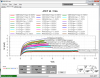
Compare 2SK30A(Y) to many-onhand Id vs Vds.png Compare 2SK30A(Y) to many-onhand Id vs Vgs.png
 
yeah, i can see without the overlaid graphs those are not a good match. Way different pinch-off and Idss (and other specs probably off due to different applications in mind).

Your Idss for the 2sk30A seems to be in line with what was discussed here (1.2-3mA). But something funny is going on. Your Vgs_off is around -1V which is okay, but the Vgs_on is +0.2V which seems weird to me. This can be seen the Id vs Vgs too. The tester should not be putting +ve values across Vgs for this type of transistor - this can result in junction damage. It's also a bit wierd that the curves go nice and smooth beyond 0V to 0.2V without any saturation of the current; it's almost like the apparent voltage has a DC error of about >0.2V? If so it means your Idss might actually be a bit higher than 1.3mA but more like 2mA.

Tester/testing issues aside, yes, you need to find a different sub. As others have mentioned it doesnt' need to be exact, but look at your schematic and make sure you device and handle more than the voltage across Vds. And find something with Idss more in the range of 1-3mA and Vp in the 1V range. How about something more like the LSK846. Vgs_off is quoted as -0.2 to -2 V and Idss of 1.5 to 15mA (5 mA typical). I bought for of those previously and have date, but haven't plotted it... i will in my other JFET thread (since I'm looking at single channel JFETs over there as well as dual). I got typical values of 0.7V pinch off and Idss of 2.5 to 3 mA for my LSK846 devices. That might do the trick?
 
Last edited:
This tells me:

  1. I have no idea how to properly find JFET replacements
  2. I have no replacement JFETs onhand that will perform similarly to the 2SK30A-Y

I guess I'll just order one of every JFET at Mouser, run the curves, and hope one is more-similar to the original 2SK30A-Y
AND order a few sets from various iffy vendors on the big auction site... and wait to see which if those, if any, are close.

View attachment 891224 View attachment 891225

Don't just order a random bunch. You will be able to find a suitable low-noise N-JFET that is more suitable than some random JFET designed for random application. I'm just focusing on Idss and pinch-off voltage on your post because that seems way off from your originally proposed sub, but as Alan implies, there might be a lot more to it than that in terms of other required specs. I think something like the LSK846 (or similar, with appropriate matching Idss and pinch-off voltage; they have a bunch of related models at LIS) will be more in the spirit of the 2SK30A circuit applications than many of those random ones on Mouser (this is not to say you will not find a good match there, but I wouldn't go about it in a random fashion). I mainly got into looking for replacements for the dual JFETs as they are hard to come by, but with the single JFETs there might be more options that those AK members with much more JFET (such as Echowars and others) that I might suggest.
 
Last edited:
Tester/testing issues aside, yes, you need to find a different sub. As others have mentioned it doesnt' need to be exact, but look at your schematic and make sure you device and handle more than the voltage across Vds. And find something with Idss more in the range of 1-3mA and Vp in the 1V range. How about something more like the LSK846. Vgs_off is quoted as -0.2 to -2 V and Idss of 1.5 to 15mA (5 mA typical). I bought for of those previously and have date, but haven't plotted it... i will in my other JFET thread (since I'm looking at single channel JFETs over there as well as dual). I got typical values of 0.7V pinch off and Idss of 2.5 to 3 mA for my LSK846 devices. That might do the trick?

Thanks very much for the detailed reply. For the limited amount I understand, it sounds like your LS846 recommendation should be close. I'll buy a set of those and run them through the test. Any recommendations on sources for the LIS devices? The only one I can find online here in the States is Trendsetter and they want $4 each (which is OK) but $20 in cheapest shipping.

The application for this 2SK30A-Y is the first stage in the control amp on a SX-626:

Pioneer SX-626 control amp AWG-008 schematic.png

If I were reading this thread and didn't have the benefit of you fine AK'ers chiming in and helping me in near realtime, how might I dissect the schematic and the measured values and apply your advice? The way I read the above schematic is "expect that Q2 will get a supply voltage of 21.6V to the drain and that should yield 5.4V at the source." I understand I'm not reading this perfectly, but perhaps this can help me test replacements.

Would the following be a better approach?

  1. Take the known part (2SK30A-Y in this case) and find its Idss and pinch-off voltage from its datasheet
  2. Look for a few other JFETs with similar Idss and pinch-off voltage from their datasheet
  3. Test for similar operation (compare original device and replacement candidate) in a test rig:
    1. Get the operating voltage of the test rig close to that of the schematic's depicted normal operation
    2. Then measure the resulting voltage across a pair of test resistors (see the below link's spreadsheet)
    3. Let the spreadsheet calculate the Vgs0 and Ldss
    4. and then type in the desired I_ds to have the spreadsheet calculate the transconductance at that drain current
    5. Then repeat for the few replacement candidates and select the one most-closely matching the original device's transconductance at that drain current
JFET "super-matching" test rig and spreadsheet here: http://www.diyaudio.com/forums/blogs/rjm/1326-matching-jfets.html

Does that approach sound like a viable way to select a well-matching device?
If so, what would one do to choose a desired I_ds to plug into the spreadsheet?
 
Okay, with the schematic you see that you have Vds of about 16V (note your tester was testing at <10V; doesn't make much difference in this case, but might for other devices). The 10k and 3.9k resistors set those 21.6V and 5.4V. Ideally, i would test the 2sk30A under similar settings in my test circuit with 2 DC power supplies - I really don't trust the tester results, but you can probably accept them as about right, keeping in mind +/- 70% on current (and/or 0.2V Vgs shift) (and similar level of uncertainty for transconductance) for the 2SK30A data you posted above. Ok moving on, keep in mind that Alan0354 is right that this is all a bit of a joke if we don't know which specs of the 2sk30A the designers 'needed'. And, we can't easily measure some of the important specs like capacitance. Okay, looking at the schematic/application, as expected we want low-noise (and probably low-capacitance, although we don't know 2sk30A capacitance values). I think you steps look good. as you say, (1 & 2) find reasonably similar values of Idss, Vp (and I would add transconductance), with a focus on low-noise/low-capacitance devices. Regarding your step (3), I think you could simplify; I think you could skip the test rig and just measure with your tester (unless you have all of the gear and DC power supplies etc etc (having proper variable DC supplies is going to much testing much simpler, but not worth the expense over your tester unless you have other uses for the power supplies)). it might be worth setting up the rig with DC power supplies but using the 9V battery and resistors is putting you in a similar position of the tester with limited power supply capability (for example your pioneer using 16V for Vds). So I would just take Ids and transconductance from your tester and do (3.5) on a few devices of same model (e.g. LSK846) until you find one with nice values (the range on same model JFETs is huge), and then move onto another model (chosen by steps (1 & 2)) if that doesn't work out.

Regarding the LSK846 and other LIS transistors, the way i bought them was directly from Linear Integrated Systems. They were perfectly happy to sell me small numbers of items. Yes, the cost is about $4 per piece (from memory) for the single JFETs but I do remember shipping being was very reasonable. (Again, there may be other suitable candidates available on Mouser but I don't know which particular models. All I know is Linear is the only gig in town making the dual JFETs I wanted, and I grabbed a few single JFETs and they seem to be very good quality/specs)
 
I think you steps look good. as you say, (1 & 2) find reasonably similar values of Idss, Vp (and I would add transconductance), with a focus on low-noise/low-capacitance devices. Regarding your step (3), I think you could simplify; I think you could skip the test rig and just measure with your tester (unless you have all of the gear and DC power supplies etc etc (having proper variable DC supplies is going to much testing much simpler, but not worth the expense over your tester unless you have other uses for the power supplies))

Terrific. Thanks! I've got the gear to test (more than one linear regulated variable power supply in the 1-50V range), so I'll give that a go.

Why two supplies, though? I understand supplying the same voltage as the Pioneer schematic (21.6V to drain and ground to source), but you're saying I should test with a second supply as well? You mean apply a second voltage, 4.2V, to the gate while under test? I was thinking the drain and the gate would both get the 21.6V supply.
 
Terrific. Thanks! I've got the gear to test (more than one linear regulated variable power supply in the 1-50V range), so I'll give that a go.

Why two supplies, though? I understand supplying the same voltage as the Pioneer schematic (21.6V to drain and ground to source), but you're saying I should test with a second supply as well? You mean apply a second voltage, 4.2V, to the gate while under test? I was thinking the drain and the gate would both get the 21.6V supply.

You can measure Idss with one DC source to apply the voltage Vds. However, to learn Vgs_off and also see performance including transconductance below full throttle, you need a second DC source between source and gate to control Vgs (without this, i.e. Vgs = 0V, the throttle is full open). Google around JFET testing and you will find some schematics, if not let me know and I will sketch.

Your schematic shows Drain at 21.6V and Source 5.4V. Do not set Gate to same voltage as Drain. Gate should be set to Source (which would be Vgs = 0V, open full throttle) + some small voltage upto V_gs_off typically in the range up to a couple of volts. (BTW, I would just set Drain to about 16.2V and Source to 0V (unless you have the resistors and replicate the conditions exactly, but i don't think it is important))
 
Last edited:
...............

  1. Take the known part (2SK30A-Y in this case) and find its Idss and pinch-off voltage from its datasheet
  2. Look for a few other JFETs with similar Idss and pinch-off voltage from their datasheet
  3. Test for similar operation (compare original device and replacement candidate) in a test rig:
    1. Get the operating voltage of the test rig close to that of the schematic's depicted normal operation
    2. Then measure the resulting voltage across a pair of test resistors (see the below link's spreadsheet)
    3. Let the spreadsheet calculate the Vgs0 and Ldss
    4. and then type in the desired I_ds to have the spreadsheet calculate the transconductance at that drain current
    5. Then repeat for the few replacement candidates and select the one most-closely matching the original device's transconductance at that drain current
JFET "super-matching" test rig and spreadsheet here: http://www.diyaudio.com/forums/blogs/rjm/1326-matching-jfets.html

Does that approach sound like a viable way to select a well-matching device?
If so, what would one do to choose a desired I_ds to plug into the spreadsheet?

1) Why are you looking for Idss and pinchoff voltage? You are not operating on either condition, according to the schematic,On Q2, Vgs=5.4-4.2=-1.2V. You are operating at normal operation. That's the reason I said it before why are you worrying about the Idss and pinchoff voltage.
2) I would look for a FET that is has Vgs=-1.2V at Id=0.4mA. This is from calculating the current through R10( 10K at the drain of Q2).

I attached your schematic with the calculated current in red. It is a simple exercise of V=IR using the voltage given at each point. Q2 and Q4 forms a common two gain stages with negative feedback through R14. The gain of this amp is approx R14/R8 +1 which is 8.2K/3.9K+1=3.1. The exact bias is not that important. The exact voltage is not that important. The only point it's important is the voltage at the drain of Q2 or the base of Q4. You don't want to be over 22.5V. This has to do with the range of output swing. If the voltage is too high, the signal will clip on the positive swing.


FET bias.JPG

Is this the real circuit you are using and to replace Q2? Or this is another exercise? If this is an exercise, this is a bad design. All the bias points relies on the Vgs of the transistor Q2. If Vgs change, it will upset the whole balance, it will change every single voltage. This is a single ended amplifier, distortion is going to be high. I use this circuit in a RF design where distortion is not important and is a very simple and cheap way to get a feedback amplifier of quite high frequency. Current through Q2 is very low, I would use at least 1 to 3mA. I would set the voltage at the drain of Q2 at about 16V to get maximum swing to avoid clipping and lower distortion because distortion rises as you swing close to the limit ( in your case is towards 25.5V)

You want to match the circuit, the most important thing is to match the voltages, which has a lot to do with the Vgs, NOT the Idss and pinchoff voltage.

Transconductance is not important. This is a feedback amp, it will compensate.

If this is just an exercise, forget using discrete FET, there are good opamps that distortion is religiously low. Want FET input, get the OPA2604. This must be some really old design from the 70s!!!
 
Last edited:
1) Why are you looking for Idss and pinchoff voltage? You are not operating on either condition, according to the schematic,On Q2, Vgs=5.4-4.2=-1.2V. You are operating at normal operation. That's the reason I said it before why are you worrying about the Idss and pinchoff voltage.
2) I would look for a FET that is has Vgs=-1.2V at Id=0.4mA. This is from calculating the current through R10( 10K at the drain of Q2).

I attached your schematic with the calculated current in red. It is a simple exercise of V=IR using the voltage given at each point. Q2 and Q4 forms a common two gain stages with negative feedback through R14. The gain of this amp is approx R14/R8 +1 which is 8.2K/3.9K+1=3.1. The exact bias is not that important. The exact voltage is not that important. I only point it's important is the voltage at the drain of Q2 or the base of Q4. You don't want to be over 22.5V. This has to do with the range of output swing. If the voltage is too high, the signal will clip on the positive swing.


View attachment 891821

Is this the real circuit you are using and to replace Q2? Or this is another exercise? If this is an exercise, this is a bad design. All the bias points relies on the Vgs of the transistor Q2. If Vgs change, it will upset the whole balance, it will change every single voltage. This is a single ended amplifier, distortion is going to be high. I use this circuit in a RF design where distortion is not important and is a very simple and cheap way to get a feedback amplifier of quite high frequency. Current through Q2 is very low, I would use at least 1 to 3mA. I would set the voltage at the drain of Q2 at about 16V to get maximum swing to avoid clipping and lower distortion because distortion rises as you swing close to the limit ( in your case is towards 25.5V)

You want to match the circuit, the most important thing is to match the voltages, which has a lot to do with the Vgs, NOT the Idss and pinchoff voltage.

Good stuff Alan. I was definitely lazy not to post a similar pic.
 
To simplify the circuit to explain a little better how this circuit works. see the attached image.

Fig.1) I drew the circuit with the feedback resistor in RED. I simplified a little by putting R12 to the +V to make it a little clearer. If you ignore R14 ( in RED), this is just a two stage amp where the first common source stage formed by Q2 and common emitter stage formed by Q4. Forward gain is gain of the first stage times the second stage. (If you can follow, the gain is (R10/R8) X (R16 X r'e). Gain of the first stage is R10/R8= 2.56. r'e is the emitter internal resistor of Q4. C8 essentially shorted out R18 to increase gain of Q4. r'e is 26mV/(emitter current) = 26mV/2.2mA=12ohm. So the gain of Q4 is R16/r'e = 10K/12=833. So total gain is about 2.56 X 833 =2132. This is the open loop gain or the forward gain. If you don't follow this, it's ok)

The R14 is the feedback resistor. If you put that in, it creates a feedback circuit like the simple opamp circuit shown in Fig.2. The gain is R14/R8.


The rest of the circuit is just a way to set up bias.

FET bias 1.jpg

As I said, this must be a really really old circuit, this is not a good circuit for hifi. Old style design tends to make one part affecting the other part and they tuck and pull each other. That's where I said in many posts ago that a good design should not depend on the parameter of the component as much as possible. In this circuit, all the bias depends on the Vgs, which is not very good. As you can see, the two stages are just common source and common emitter stages, they are single ended circuit, not balance type, distortion is very high. Even with feedback, you still have a lot of distortion.

Since the FET is biased on and the Vgs is about -1.2V, you are not operating anywhere close to Idss ( Id at Vgs=0V) and pinchoff ( Vgs at Id=0) region. Those parameters are irrelevant. You make it very hard for yourself trying to match those for nothing.

As I said, all you need to look for is Vgs of about -1.2V at Id=0.4mA if you want to copy exact voltages of the circuit. I would not even worry too much. I would like to have the drain of Q2 a little lower like 16V to optimize the swing in both direction.

There you have it.
 
Last edited:
To simplify the circuit to explain a little better how this circuit works. see the attached image.

...

As I said, this must be a really really old circuit, this is not a good circuit for hifi.

...

There you have it.

Awesome. Thank you!

Yep, you called it. This is a vintage Pioneer SX-626 receiver from the 70's. I'm looking to find a modern replacement for that one pair of JFETs and that's it. I'll try your layout.

Thanks again,
Doug
 
Speaking of fancy testers.....

I would like to know if my 2SK97s are bung or not - I will build a basic N-type tester this weekend based on some internet diagrams. I followed the procedure in post #2 here:

https://pinside.com/pinball/forum/topic/how-to-test-a-fet-transistor

and I got open circuit between gate and drain/source on both polarities of the meter leads. However I did get readings of around 100ohm between drain/source on both sides (after shorting the pins before testing).

I also thought I could measure this in my basic little component tester and got this for both sides. It has correctly identified the type of component, so it seems it may be on the right track......How does this look - OK, bad, inconclusive? Thanks!

20171115_174656.jpg
 
Last edited:
giphy.gif
 
Great work!
Has anyone tried the LSK389 for Sansui AU-517?
I'm not very well versed in electronics and I gave my AU-517 away to be repaired. Now they tell me that both 2SK97 are not working any more. And there is nothing they can do for my AU-517. They have a good reputation, so I guess it is true.
My Sansui is still with them, I found some pictures of the 2SK97 in this report: Sansui AU-517 Complete Restoration.
There it is a Sony K97 JD21.
Is the LSK389B still the way to go?
Perhaps they are willing to try or I would need to find another repair shop. Ending up with a nice paperweight would be really sad.
 
Back
Top Bottom