Hello all. I’ve inherited a broken SP10. First thing I need is a very clear picture of the underside of power supply PC board. Especially the area where the chips are. Pretty bad repair was made there, chips replaced, but some of the traces are gone. I will need to restore those. Would really appreciate if someone could send me a good picture. Thx in advance.


You are using an out of date browser. It may not display this or other websites correctly.
You should upgrade or use an alternative browser.
You should upgrade or use an alternative browser.
Audio Research SP10 help needed.
- Thread starter marknoir
- Start date
-
- Tags
- audio research sp10
Register to hide this ad

ernieS
Well-Known Member
I bit the bullet and sent my SP9 back to ARC for repair. Bill was $700, but the unit is now flawless, new tubes. I got mine in a trade, one channel out.Hello all. I’ve inherited a broken SP10. First thing I need is a very clear picture of the underside of power supply PC board. Especially the area where the chips are. Pretty bad repair was made there, chips replaced, but some of the traces are gone. I will need to restore those. Would really appreciate if someone could send me a good picture. Thx in advance.
Thx for reply. Part of fun for me is fixing things myself, until I come to a conclusion that it’s time to give up ))). I’ve rebuilt and restored one of these before, about 10 yrs ago, from a complete basket case. ARC will probably charge about $2K to bring this one back to life…I bit the bullet and sent my SP9 back to ARC for repair. Bill was $700, but the unit is now flawless, new tubes. I got mine in a trade, one channel out.

I don't think it is too expensive to make PC boards you just need to reverse engineer the ones you have and get a new batch made. I think you might have to make a minimum, but my son did some for another project and it wasn't very expensive. Better to make new ones than use an old board that is full of lifted traces.

Is it possible to post photos of this damage? Just to see the bad repair job.Hello all. I’ve inherited a broken SP10. First thing I need is a very clear picture of the underside of power supply PC board. Especially the area where the chips are. Pretty bad repair was made there, chips replaced, but some of the traces are gone. I will need to restore those. Would really appreciate if someone could send me a good picture. Thx in advance.
Maybe it's one of those, "You think that you've seen every hack repair... but another one shows up that's even worse."
Thanks!
Over the years I recall a few that I did, not very pretty.Is it possible to post photos of this damage? Just to see the bad repair job.
Maybe it's one of those, "You think that you've seen every hack repair... but another one shows up that's even worse."
Thanks!

If the solder doesn't flow quick and smooth the first time with just a small dab, it seems like the more you mess with a joint the worse it gets. And trying to solder on a heavy gauge with a smaller wire trying to get that heavy joint hot while those small wires insulation starts melting my worst nightmare. Those old PC boards where all the ground wires land on the same spot those are tough ones for me too.
Last edited:
I’ll try to take some pictures tomorrow, if I can zoom in close enough.Is it possible to post photos of this damage? Just to see the bad repair job.
Maybe it's one of those, "You think that you've seen every hack repair... but another one shows up that's even worse."
Thanks!

Best of luck. The traces on ARC gear are absolutely horrible. If it really comes down to needing a brand new board, I would happy to help design one.
Thank you. Agree.Best of luck. The traces on ARC gear are absolutely horrible. If it really comes down to needing a brand new board, I would happy to help design one.
I think this board is restorable. I certainly would hate to replace/re-populate the whole PS board. I’d rather do some point-to-point wiring around those chips. I can trace according to schematic, but a good photo would save me a ton of time.
Here it is:Is it possible to post photos of this damage? Just to see the bad repair job.
Maybe it's one of those, "You think that you've seen every hack repair... but another one shows up that's even worse."
Thanks!
Attachments
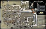
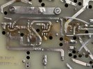

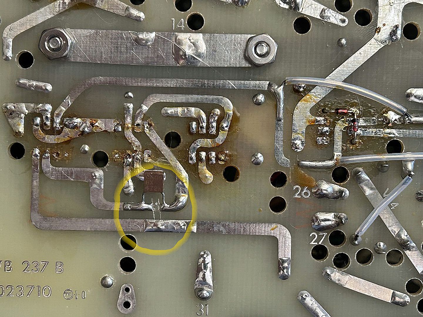
This doesn't look correct.

And that’s why I need a good picture of what it SHOULD look like.
This doesn't look correct.
Actually I looked at the schematic, and this is - surprisingly - correct. I think this was a mood to later units. Everything here looks correct and actually connected, except the TL071, where the slides in schematic go from pin 2 to pins 4 and 7, and here they go from pin 1 to 4 and 8. I have to look into that.
This doesn't look correct.
The catwhiskers of the solder seem to be shorting across that cap.Actually I looked at the schematic, and this is - surprisingly - correct. I think this was a mood to later units. Everything here looks correct and actually connected, except the TL071, where the slides in schematic go from pin 2 to pins 4 and 7, and here they go from pin 1 to 4 and 8. I have to look into that.

ARCDB has a manual with two different schematics in it. One is hand-drawn for Mk I, and one computer-generated (they say - “redrawn” in 2003) for Mk II. No incremental changes are shown in schematics, but it dyes list all revisions by number.I don't suppose the ARC DB has info on the revisions or schematics showing the various changes?
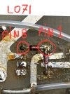
I think I found at least one problem: L071’s supporting circuit’s diodes are not soldered to correct pins. Main complaint was that the muting circuit won’t open after previous repair, which involved replacement of a blown VR1 regulator and its L071 feeder. Well, muting circuit in this preamp is not only a time-delay. It also protects outputs if something is wrong. The diodes supposed to go from pin 2 to pin 4 and pin 7. Instead they are soldered to pin 1 and one to pin 8, both are not used on L071.
Attachments
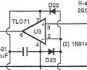
In my opinion, there is a lot of questionable work in those photos. You have to ask: 1.) Why so much work? and 2.) Are they hiding a deeper, maybe inherent problem of the unit?So it looks like this crazy connection destroyed TL071, and possibly more. So I have to go through this carefully, but I think this is the culprit. I still do wish I had a very clear picture of this PCB…
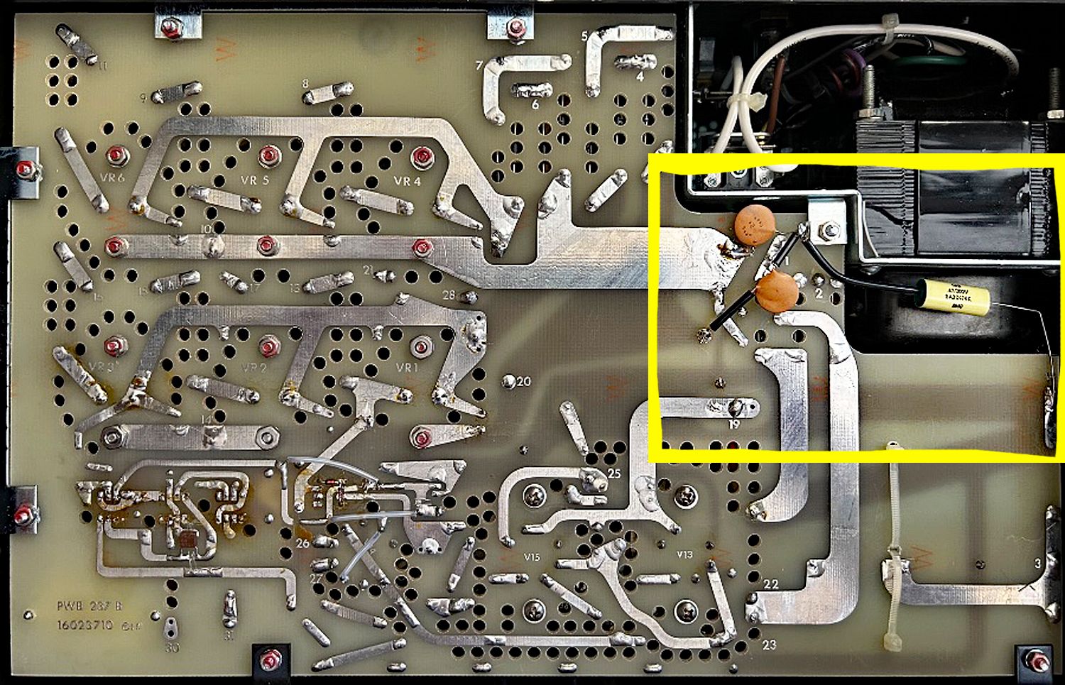
I was able to restore all the damaged traces, replaced some dead parts. Raised it in my variac today. Nothing burned )))). All transformer windings produce correct voltage; filament vintages are correct as well. The problem is high voltage. It begins to go up, but at about 220v there’sa loud relay click and voltage drops down to about 90, and starts there. Auto mute keeps on blinking. I don’t understand yet what its going on, and also can’t find any protection relays yet. Seems that the auto-mute protection kicks-in because high voltage is off? Another mystery )))
PS found another broken trace. Will continue tomorrow
PS found another broken trace. Will continue tomorrow
Last edited: