• The move to the new server is done. There are some software and database maintenance updates in process. This has us passing the hat around to help out. We appreciate any donations. Seriously, even a dollar helps. The payment page may be found here - https://www.audiokarma.org/support.html

CA-1000 Rebuild Issues

jandajr

Active Member
On an earlier thread concerning this CA-1000, I needed help gathering parts.
I thought that I should start a new thread seeing that it concerns operation issues on my CA-1000
This non-working CA-1000 was an online purchase that had several attempts of repair.
I could not attempt to turning it on, it was a total wreck.

I Completely rebuilt:
• Power Supply Board
• Main Amp Boards

I Re-Capped all remaining boards.
Replaced:
• Fusible Resistors
• Power Switch
• Filter Caps
• Class A/AB Switches
• Dissembled and cleaned all switches/controls

When I put it on the DBT, it failed. Took out R625 and R626 on the (right) Main Amp board.
I replaced the burnt resistors and checked and tested all the Diodes, Transistors, Resistors and Capacitors.
Put it back on the DBT, failed again. I shut it down before could do any damage to the resistors.
I’ve re-tested every component on this board. I can’t find anything.
I removed the +50 lead from the (right) main board, and it passed the DBT.

Any suggestions what to look for would be greatly appreciated.
 
Register to hide this ad
Pull out your magnification and start looking for solder bridges. Sounds like you have a short between traces. When doing lots of solder work on a board, this is something to be wary of.
 
  • Like
Reactions: mbz
Great call. I've been looking at the front of this board till I'm blue in the face. But not the backside.
I'll update as soon as I can.
Thanks!
 
R633,4 emitter resistors ok?
Did you replace VR603? VR open?
Same behaviour when Operations=class A?
Did you clean the operations slide switch for pins A,B,C,S? Would be nice to know Vdc at pin C, expect
about 4Vdc(normal) and 2.7Vdc (Class A)

Should be 1.2Vdc across R625,6 so 3mA, a solder bridge would help.
 
mbz
R633,4 emitter resistors ok? YES
Did you replace VR603? VR open? YES replaced with Bourn
Did you clean the operations slide switch for pins A,B,C,S? Yes Disassembled and cleaned

Would be nice to know Vdc at pin C, expect about 4Vdc(normal) and 2.7Vdc (Class A)
Same behaviour when Operations=class A?
Should be 1.2Vdc across R625,6 so 3mA, a solder bridge would help.

Concerning the balance of the questions above, I have this question:
I can only run the amplifier for a second, before I start to smoking R626. (off the DBT)
Is that enough time to get the correct voltage?
 
I can only run the amplifier for a second, before I start to smoking R626. (off the DBT)
Is that enough time to get the correct voltage?
I wouldn't risk the damage, wait on this measurement.

With amp powered off/unplugged measure resistance between right channel pins
B&C... approx 0.5ohms
B&S... approx 470
C&S... approx 470
A&B, A&C, A&S about 1.5k-3k
Post actual measurements

Measure resistance between R625 or R626(either side) and chassis/GND
Wanting to see hundreds of ohms(C615?)
 
mbz

B&C 0.4 Ohms
B&S 474 Ohms
C&S 474 Ohms
A&B 110 Ohms
A&C 110 Ohms
A&S 584 Ohms

R625 21.7K Ohms
R626 21.8K Ohms
C615 1.6K Ohms
 
A,B,C,S resistances appear ok, VR603,4 appear set to near minimum.

R625,6 resistance to GND appear a bit high however more importantly no
low resistance path to GND(solder bridge?). So it's the voltage differential
between TR609e and TR610e that appears out of whack.

Have you tried DBT power up with F601,2 removed and +50 reconnected?
 
Yesterday before I started to check the resistor values, I removed VR603 to check it outside the circuit.
Soldered it back in and then checked the resistances you requested.
Ok, this is where it gets strange.
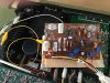
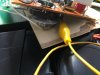
This morning I decided to just go for it. As you can see I hooked up the collector (on the output transistors) to ground on the left channel heat sink.
Put it on the DBT and powered it up.

Past the DBT and a couple of seconds later the protection relay kicked in.
As I let it run for a full minute. Using my Infrared Thermometer I checked the resistors R625,26 and other resistors and transistors.
Nothing, Seems to be ok.

Seeing that the only thing I touched was VR603, I might have had a bad solder joint on that trimmer.
Ok, So do I go the next step and remove the DBT and go for broke?
Are there any measurements I should look for, before I try to make adjustments to each board?

Or Am I being over optimistic?


IMG_1859.jpegIMG_1860.jpegIMG_1861.jpeg
 
The DBT dims in both A & AB modes.
I put the board back on the heat sink and re-pasted the output transistors.
Re-tested it again and let it run again for about a minute.
Again, no pops smoke, sparks.

I think it's time to put my multimeters on it and try to dial it in according to the service manual.
 
Before going off of DBT, consider checking to see that the trimmers are responding to adjustment. Set bias fairly low if they are, then proceed to go off DBT and adjust to spec.
 
I Checked the trimmers. No response on VR 603/604
Decided to go off the DBT anyway. Flipped the power switch with operation switch in Normal setting.
Relay clicked everything seems OK.
Let it run for a few minutes then set VR602 to 15V on both channels.
Then I set VR601 to 0.01V on both channels.
Still no response on VR603/604 in both Class A/AB in both channels.:wtf:
 
Forgot to mention that the voltage reading on VR603/604 is 0.01 on both settings and channels.

If that means anything.
 
Forgot to mention that the voltage reading on VR603/604 is 0.01 on both settings and channels.

If that means anything.
Did you install new trimmers, or are vr603/4 the originals? Sometimes the new multiturn ones get rotated "too far" and won't adjust anything until you spin them in the correct direction a bunch of turns.
 
Yes I replaced them with the bourns Multi turn units.
I tried turning them a bunch in both directions.
I'm hoping that it's not the slide switch. I dissembled and cleaned it. I've done many of those without an issue. Maybe my luck ran out.
 
Maybe a problem with R627,8. What voltage are you seeing at TP3 to GND. Repeat for TP4 to GND. expect +/-100 or so mV.
Resistance check R627,8, amp powered off, approx 4.7 ohms. Also check R621,2 (680) fusibles in some units and possibly replaced as per post #1.

Monitor voltage at pin C while adjusting the VR, wanting to see about +1.1Vdc Does this voltage change while adjusting the VR?
Likewise voltage to GND at R617 (the 470 ohm in front of bias transistor) should vary with VR adjust

Check voltages to GND at each of the power amp fuses, expect about +/-50Vdc(Normal) and +/-20V(Class A)
 
mbz
I started by going back to your earlier post.
The two questions you ask (see below) I was not able to do at the time because of the smoking resistors.
Now that we are passed that, I took the reading you requested.

Did you clean the operations slide switch for pins A,B,C,S? Would be nice to know Vdc at pin C, expect
about 4Vdc(normal) and 2.7Vdc (Class A)
Should be 1.2Vdc across R625,6 so 3mA, a solder bridge would help.

Pin C: Normal .73 Vdc
Class A 1.85 Vdc
R 625: .193 Vdc
R 626: .312 Vdc

This is nuts, the reading don't make any sense. Low readings that are ass backwards.
If the operation slider switch was re-assembled improperly, could it be possibly giving me those wacky readings?
If so, is there a way to bypass the switch (in one of the setting) to see if that has any effect?
 
Back
Top Bottom