• The move to the new server is done. There are some software and database maintenance updates in process. This has us passing the hat around to help out. We appreciate any donations. Seriously, even a dollar helps. The payment page may be found here - https://www.audiokarma.org/support.html

Diode Bridge consult

oldNslo

Member
Ok, those with far greater knowledge, I have a few questions as I proceed forward with a replacement part.

The left image is from the Yamaha SM, the right is from Mouser for a DB105. The OE part is WH471700 (not seemingly obtainable) however is marked DB105 on the component on the board now.

Q1 = are these 2 electrically equivalent? Is 1 less diode just a result of getting smarter over the years?
Q2 - Is the right image "tested" in the same manner of a bridge diode? (ie reversing the test leads)
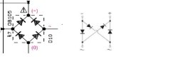
DB105 examples.jpg

Q3 - I'm presuming I need to get my DC leg orientation correct, and would be indifferent to the AC leg orientation. Is this correct?

Thanks in advance!
 
Last edited:
Register to hide this ad
both of these are 4 diodes, not sure what you mean about one less diode.

The one on the left is drawn wrong. This wouldn't produce a workable bridge if the AC is fed in at 12:00 and 3:00. If you feed in AC at 3:00 and 9:00, negative would be at 6:00 and positive would be at 12:00.


diode bridges are pretty interchangeable honestly. Meet or exceed the amp and voltage ratings, and just match up the pinout. They exist in enough packages that something must exist with the same arrangement. Generally you get a square with AC on opposite corners and DC on the other opposite sides, or an inline package. Match that up to whatever your board needs.
 
Sheesh, my bad on the count. Sry. I'll review the other DB105 found on the drawing and the board and report back. Thanks for the fast response!
 
Take a picture of the board diode. That will show the package, somebody should be able to point out the markings on the diode to you (notched corner and symbols).

Of interest is why you are replacing it; is it old and tired looking or dead short. Or?
 
Those are equivalent. They're just drawn differently. If you flip one side of the right diagram then rotate 45 degrees, it's the same as the left.
 
Thanks all. Upon closer magnification of D10 and D11 (both are the same values on the parts list), they both fail the standard multimeter diode test. D10 is OL on the AC side, D11 is shorted on the on the AC side. No visible signs of trauma, and clearly marked with +/- on the unit. No board trauma anywhere. Thus these two are on my parts buy list.

I'm trying to remedy a "fail to power up", that is NOT C4 (highly discussed for Yam AV amps), C6 or C7. All those caps test the same as my new replacements, which were purchased before I removed them to test out of circuit :thumbsdown:. Even C9 (when removed) located between the power supply (T1) tests right at spec. I'm working my way back to line voltage in my testing process.

T1 is somehow putting out millivolts vs the 5.9 AC spec (attached). I'm scratching my head watching YouTubes on the testing process of prim/secondary circuits in order to duplicate results on some "parts" transformers and the one on the Yamaha board. I'm testing both out of circuit for resistance readings and bench testing the board under power and disconnected from the amp for AC readings.

So, I think I have the diode bridge under control, until I remove them for the board for final (out of circuit) testing, and seems I need to get my act together on transformer diagnostics, of which T1 (X7033A00) seems a bit elusive to find a replacement at the moment should it not be healthy.
 

Attachments

  • Yam Power supply.jpg
    Yam Power supply.jpg
    19.3 KB · Views: 13
Thanks @Warren-Oates , I figured so. Appreciated. My attention is now to solve the needed transformer output pf 5.7vac.

So, what have others done when a power transformer (on a PCB) is no longer available? A call to Yamaha offered no solutions or equivalents. I don't seem to google any specs on it, or alternate sources for X7033A00 or even locate a data sheet with this part. I see how mfgr's make obsolescence part of the business model. Ugh.

Perhaps part of the answer is the 5.7vac on the secondary, I'm presuming its 120v from line in , but have no idea on any ohm resistance or other parameters other than the obvious of size, etc.. Perhaps those will emerge once removed from circuit and I can retest then. Any guidance here would be appreciated.

Random part example from DigiKey
1790702886697.png
 
With the bridge out, ohm check the transformer secondary and see if its good. If it is, ohm check the primary and confirm its also good. A shorted rectifier with a too-big fuse could have fried the transformer.

If that checks OK, make sure the transformer actually has power on the primary side.
 
Do you have +5Vdc at pin +5M at W1 page 128 co-ordinates I8

edit any voltages on fet Q6 G/S/D?
 
Last edited:
With the bridge rectifier removed, it has one diode leg (AC to AC) that measures OL. The other 3 are OL and .502, with the 3rd being OL and .92

With it removed I do have 120v to the primary side and .622kΩ. The secondary measures 13.5vac (yikes) and 12.9Ω.
I also have 4.9vac at the +5 pin

Q6 readout attached. I must admit, I don't understand these parameters, and could not square those up with a sample data sheet (same part # 2SK3850) from Sanyo.

C6 Mosfet.JPG
 
  • Like
Reactions: mbz
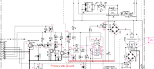
Attached relevent part of schematic.
Beyond my pay grade, maybe one of the techs can clear up?

Is this something of a poor mans SMPS?
T1 primary will only be energised if there is current flow (through bridge D10 and Q6?)
So if Q6 is incorrectly biased/no S, D current the T1 primary current stops. That's why
I wanted the Q6 gate Vdc.
 

Attachments

  • rx-v1800.pdf.png
    rx-v1800.pdf.png
    99.5 KB · Views: 19
662 ohms on the primary side seems very high if this is meant to deliver any sort of current, but I freely admit to not understanding whats going on here. I'm not used to seeing transformers with a bridge on both sides of it.

then again 13 ohms on the secondary side also seems high, but if its a weenie little transformer that may be correct.
 
With it removed I do have 120v to the primary side
Was bridge D10 removed??? this would indicate T1 is ok, also D11 probably ok.
Suggests problem is downstream loading on D10 then primary? Odd observation.

Is it possible to pull the connector on the other end of W1, ie, CB146 on Function(1) board page 122 D9
then check T1 primary & secondary voltages
 
Thanks @mbz for your continued help. It is really appreciated. I'll respond to this, along with other inquiries, in the linked thread referenced in post 16, so as to keep things tidy and close this thread out.
 
Back
Top Bottom