mcaddie7
Active Member
I want to preface this with I'm a pretty big nob and have never touched a transistor or biased anything. I have however recapped my Harmon Kardon 930 to what seems great success. There are several guides on this site for biasing this receiver but non include pictures and thus I really can't follow them. Some say have a load on the speaker terminals, some say don't (capacitive coupled?). I'd like to get a definitive guide for this receiver.
So two things:
1) I checked the DC offset on each speaker terminal and go about 120mV on each one. Is this good, is this bad, or should there be some load attached (and if so how) and how to adjust this?
2) for biasing the Output the manual states the following:

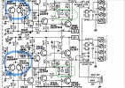
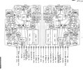
The test points are on the schematic here:
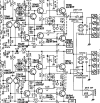
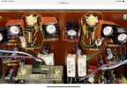
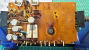
My question is, where the hell is TP1 on the actual board? Is it the yellow and purple wire that seem to serve no purpose? When adjusting this should there be a load or not?

Any help would be greatly appreciated for a begininer such as myself, as the other guides I just can't follow and want to be a sure (plus it should help future noobs when fixing this receiver).
Thanks so much!
So two things:
1) I checked the DC offset on each speaker terminal and go about 120mV on each one. Is this good, is this bad, or should there be some load attached (and if so how) and how to adjust this?
2) for biasing the Output the manual states the following:
The test points are on the schematic here:
My question is, where the hell is TP1 on the actual board? Is it the yellow and purple wire that seem to serve no purpose? When adjusting this should there be a load or not?
Any help would be greatly appreciated for a begininer such as myself, as the other guides I just can't follow and want to be a sure (plus it should help future noobs when fixing this receiver).
Thanks so much!