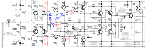
I can only offer a high-level overview and some simple observations:
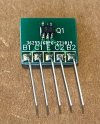
- Q406/408 and Q402/404 are the dual differential inputs using the rare and exotic uPA74V/uPA75V differential transistor pairs.
- Q410/412 buffer the input signal and set the bias for:
- Q414/416, who provide the bulk of the voltage gain.
- Q418/D418 and VR404, of course, establish temperature sensitive bias separation for the main output transistors downstream.
- Complementary Feedback pairs Q420/424 and Q422/426 provide current gain to drive the main output transistors with only one junction drop (compared to a Darlington arrangement) and, reputedly, O(10) less variation with temperature.
- Our main output pairs, Q428/430 and Q432/434, of course, are biased away from each other to reduce zero crossing distortion.
A notable feature of this amplifier is the higher voltage rails (+/-50V) applied to the amplifier before the (+/-40V) main output section, fed by a pair of slightly novel multi-tap transformers.
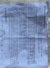
I was looking through your measurements near the bias spreader.
- One of your measurements might be off: Q414(c) reads -1.36 (close to spec) while Q420(b) reads +1.45. Those are the same node; I'm guessing the negative value is more correct.
- Q416(c) and Q422(e) are reading about a volt high, but Q426(c), which establishes the high-going main output bias, is pretty close to spec. This may not even have much of an effect, since Q422(c) and Q426(e) voltages are reading nominal, which means they aren't drawing worryingly more or less current than they should.
Wiser heads might see something more subtle...