• The move to the new server is done. There are some software and database maintenance updates in process. This has us passing the hat around to help out. We appreciate any donations. Seriously, even a dollar helps. The payment page may be found here - https://www.audiokarma.org/support.html

Is it the IC or something else?

QSilver

Super Member
I've been working on an SX-V80 I picked up a month ago or so. Giving it a recap, replacing very worn trimmers and some resistors. I finished the job and powered it on for a test to find the left channel was very weak.

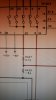
After a lot of probing, I've found that the signal remains strong all the way through the pre amp, volume control chips, op amps etc.... it's only when it gets to the final IC before being passed to the power amp section. This seemingly controls the "Simulated Stereo" feature and the subsonic feature. I have a good signal, equally comparable to the right channel, on Pin 20. The signal is still good on the Pin 20 side of R437.

On the other side of R437 and all the rest of the way to the pre amp out jacks, the signal is feeble and almost not even there....

I've tried changing R437, I've lifted R439, I've even disconnected the pre amp out jack cable from the board and nothing improves it. My next thought was to maybe consider bypassing the IC... I can get another one of these.... looks like its a TC9163N...

Just looking for some advice as I'm a bit stumped as to what to do next... I feel like I'm almost there but maybe I'm not seeing something....?

EDIT: It's probably worth noting, that the receiver had been worked on before, the Zener diodes that regulate the 16+/-VDC supplies for the logic controls looked stressed and one of them snapped when I tried to remove it (it had been refitted onto the underside of the board) I then found that there had been a burnt out resistor for that Zener which had been replaced with a 100R when it should have been 150R. I rectified this too. The voltages to the ICs and Microcomputer are at 17.5V+/- the Zeners I replaced the originals with were 16V zeners.

Everything else is working well. Just this left channel issue the seems to be centered around IC404....
 

Attachments

  • SX-V80-IC404.jpg
    SX-V80-IC404.jpg
    59.2 KB · Views: 29
Register to hide this ad
TC9163 is an analog switch which is serial controlled using the clk,data,strobe control lines.
Download the device datasheet to learn more.
The device looks to be available from some HK sources at a low cost if it turns out to be that part.
Have to wonder if it worked before you did your mods, what made it fail, if it is that part which is causing your problem.
 
It was working - passing signal correctly before I did a recap on it. As I was working through it I found a resistor that bad been replaced having burnt up (charring on the PCB). It is supposed to be 150R but has been replaced with 100R. My thinking was that this would increase the current to the zener which would be stressing it. You could see a discolouration on the PCB around the zener diodes. The replaced zener had been mounted in the bottom of the board and as I was desoldering to move it to the top of the board, it crumbled so I had to replace it. I replaced the pair.

I've been through the circuit and the only thing I found was that C417 had been mounted backwards so I rectified that but no change. I've reflowed the IC connections... could I bridge the IC? I'm not sure how else I can test it with power off. I've got the datasheet and I did start to read up.

I took some continuity readings on the IC and found that the signal path from pin 3 to the preout jacks is around 100 Ohms. I haven't compared to the right channel yet... Though there is also a near short to ground on pins 5 and 19 of the IC...
 
Unless the new zener's were not correct. The input to all the CMOS chips is 17.5VDC dual power supply so its over 34VDC which is the max rating for the chip... The old Zeners were RD16EB which I replaced with a 16V Zener. Maybe this would be the cause of a failure?
 
One possibility is the zeners smoked causing an over voltage to IC404. You can easily bypass the part. Pull the conn going to the pre-out/power-in jacks and wire to the dc blocking ecaps that feeds IC404. If IC404 has an input short then you will have to isolate it by lifting one leg on the input coupling ecaps.
 
I'll give that a try but it seems that the zeners are okay at the moment but they read out at 17.5VDC... so perhaps I should get some lower voltage zeners to lower the voltage down to 16V. 17.5V I think just goes over the IC's maximum voltage rating...
 
I replaced IC404 this week but no change at all. The left channel matches the right channel signal right up until it passes through R437. At that point, the left channel signal all most vanishes... that leaves the new chip and R439 in the path.... is it possible there is some leakage to a nearby ground trace in that path? I had a lot of problems with the left output of the pre amp showing a short to earth until I cleaned the board....? I'm very confused... any ideas? :crazy:
 
have a look around q401 q402 .
are there any more of those switches ?
not being able to see the whole schematic isnt helping
 
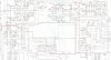
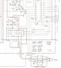
The schematic is really big but I've uploaded a little bit more.... I could try lifting C421? That would disconnect Q401 and Q402 from the circuit? There are more switches further back in the circuit and they seem to be working.
 

Attachments

  • SX-V80 Schem.jpg
    SX-V80 Schem.jpg
    77.7 KB · Views: 9
Q401 and Q402 looks to be the "Simulated Stereo" circuit. IC404 switches the output of that circuit on and off along with the subsonic filter and the original "clean" signal.
 
the q401 q402 circuit is the only thing that can take the signal down apart from a solder short or cracked trace
 
I pulled C421 which made no change to the behavior. However, if I then switch on simulated stereo, the signal disappears from the left preamp output but gets stronger on IC404 Pin 3. At the point, the signal is at around 1/3 to 1/2 of the right channel....
 
I'm lost... only thing I can think of is if the signal is shorting to a ground somewhere or being lost through a spec of solder on top of a trace....?
 
I just picked up one of these up today! Let me know if there is anything I can do to help. Mine seems to work as it should.
 
Get a 12cm 12V fan, and small fan controller and set it up blowing air onto the power supply board - parts of it get to over 100°C! It will eventually cook itself to death. It will fit between the power amp heatsink and the power board.
 
Well, I dug this out of the pile last week and I've just repaired the fault. It was a little bit of a lengthy process and in the end it wasn't the IC at all.

Firstly, I replaced the Zener diodes that supply power to the ICs on the Audio Board with 15V zeners. As it turns out, Pioneer run these ICs at +/- 16V (32V Potential difference). I looked up the data sheet for some of these ICs (Toshiba TC9163) and the absolute maximum rating is +/-15V (30V potential difference) so these were running slightly over their ratings.

I decided to drop the voltage to around 15V instead of 16V as this is simply derived by two Zeners on the Audio Board behind two 150 Ohm resistors. I did this as a precaution and to try and prolong the life of the ICs.

Next I looked into the problem again. After the 4.7k resistor, there was no signal on the left channel. I figured that it must be getting bled off. Measuring the resistance on Pin 5 (the output of the IC to the pre-amp out jacks) On power up, the resistance to ground drops down to 95 Ohms so I figured something was being told to conduct to ground (maybe one of the switches in the IC). This is all computer controlled so I cant stop it doing that.
IMG-20180330-WA0006.jpeg
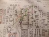
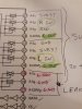
I printed the x-ray schematic and started to plot where the signals were going and which pins were doing what. IC404 is the last switch before the pre-out jumpers and this allows the computer to switch the signal routing through either the "Simulated Stereo" feature, and/or the "Subsonic Filter". This means the signal passes through one set of switches in the IC, back out and then it is looped back in again through more switches, then off to the pre-amp out jacks.
20180406_213756.jpg
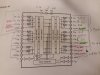
Next, I looked at the configuration of the actual IC. The datasheet showed me a good layout of the switches and allowed me to map out where the signal was going and HOW it could be switched and routed.
20180406_213804.jpg
You'll see that some banks of switches do not need to be used and so they have all been connected to ground to stop them interfering.

This is when I noticed Pin 19. On the schematic, you can see that the output of the IC to the pre-amp out jack is through Pin 5 AND Pin 19.

As it turns out, Pin 19 is connected into the audio path and can route audio to either Pin 17 or Pin 18 which are both GROUNDED.
20180406_213813.jpg
I then soldered Pin 19 and hey presto! Balanced audio output on both channels!

So the key thing to remember is, if you see Pin 19 unsoldered in one of these, Leave it unsoldered or unsolder it. I used solder wick to remove it quickly and cleanly.
 
Last edited:
Back
Top Bottom