• The move to the new server is done. There are some software and database maintenance updates in process. This has us passing the hat around to help out. We appreciate any donations. Seriously, even a dollar helps. The payment page may be found here - https://www.audiokarma.org/support.html

JVC M-7050: restoration and revisions

Jcandy

New Member
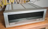
Hello all. I've finally started a JVC M-7050 restoration, and have decided to document the process here because I anticipate a long and challenging journey. The unit came from eBay and, luckily, was not damaged during shipping (in contrast to a JVC P-3030 received some weeks ago that was badly damaged in shipping).

The exterior is in nice condition and I have high hopes that the gigantic VU meters will function correctly.
 

Attachments

  • m-7050.jpg
    m-7050.jpg
    103.7 KB · Views: 49
Register to hide this ad
I had an earlier helpful exchange with @GD70 where we discovered some parts variation between our units.
  • I have 4-leg bridge rectifier which corresponds to the schematic (see images); he has PCB riser with 4 diodes
  • We both have 330uF caps at C509/C510, schematic says 220uF
  • I have no caps at C507/C508, schematic says 0.01uF, parts list says 0.1uF
  • I have 1uF caps at C511/512, schematic says 0.47uF, parts list says 2.2uF
 

Attachments

  • bridge.jpg
    bridge.jpg
    184.3 KB · Views: 29
  • schematic.png
    schematic.png
    290.8 KB · Views: 29
Hello all. I've finally started a JVC M-7050 restoration, and have decided to document the process here because I anticipate a long and challenging journey. The unit came from eBay and, luckily, was not damaged during shipping (in contrast to a JVC P-3030 received some weeks ago that was badly damaged in shipping).

The exterior is in nice condition and I have high hopes that the gigantic VU meters will function correctly.
That amp looks mint!
Looking forward to the resto updates!

Cheers, Glenn
 
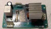
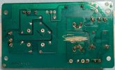
Hi Glenn. The outside is definitely in nice shape but the inside is another story. Chapter 1 of the story is the Power Supply Circuit board. A missing resistor and some bizarre etching courtesy of the previous tech (see images).

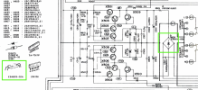
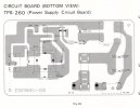
Note that the schematic for this board is different in my service manual than it is in the HFE service manual (see images), even though the manual dates are the same (July 1979). Do you have tps226 or tps260?
 

Attachments

  • tps226-top.jpg
    tps226-top.jpg
    103.5 KB · Views: 30
  • tps226-bottom.jpg
    tps226-bottom.jpg
    107 KB · Views: 30
  • schem_tps226.jpg
    schem_tps226.jpg
    72.7 KB · Views: 26
  • schem_tps260.jpg
    schem_tps260.jpg
    79.3 KB · Views: 28
So here is the problem
  • The factory outputs are two pairs of 2SC2526(G)/2SA1076(G) per channel (JVC power cascode)
  • Left channel is original and all good. Gains of outputs are closely matched (68,69,56,66)
  • Right channel has non-original 2SC2565/2SA1095, with one 2565 sorted and one 1095 shorted
  • Gain codes of the non-originals are off (service manual says 2565(O) and 1095(O) are acceptable replacements)
I think finding 2526(G)/1076(G) or 2565(O)/1095(O) online is hopeless. The best modern replacement option seems to be MJL3281A/MJL1302A, but I suspect the gains must be closely matched and in the range 55-75. Emitter resistors are 0.47 Ohms and are connected to thermistors, so I am afraid straying too far from HFE=70 will cause problems, and decreasing emitter resistor values seems complicated. Thoughts?
 

Attachments

  • outputs.jpg
    outputs.jpg
    96.5 KB · Views: 25
  • schem_output.png
    schem_output.png
    193.7 KB · Views: 24
  • heatsink.png
    heatsink.png
    140.5 KB · Views: 24
Isn't one of the purposes of the emitter resistor to make it not as critical to match the gain of the output transistor when in parallel?
 
@redk9258 yes, that is correct. However, I do not really understand the M-7050 topology so worry about the downstream effect on the thermal protection and/or bias. My hope is to find modern replacements in the same gain range as the originals.
 
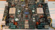
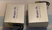
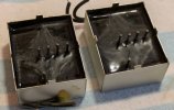
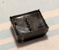
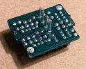
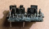
Super-A problem: the 5-pin Super-A block on the channel (R) with shorted outputs measures differently than on the presumed-good left channel. Specifically I use resistance or diode mode between the pins (out of circuit) and while some pin-to-pin measurements are the same, others are different. Like with many other parts on the M-7050, there appear to have been revisions on the Super-A blocks (TAD-198A, TAD-198B). @GD70 for example has "open" blocks whereas mine are completely sealed (see photos). Every other issue I have with this restoration seems solvable, but I have no idea how to proceed here :(
 

Attachments

  • SuperA-onboard.jpg
    SuperA-onboard.jpg
    121.9 KB · Views: 27
  • SuperA-case.jpg
    SuperA-case.jpg
    77.6 KB · Views: 27
  • SuperA-pins.jpg
    SuperA-pins.jpg
    83.1 KB · Views: 27
Looks like the A-X5 has a discrete Super A circuit. The SM has a circuit description and schematic. My eyes are crossed trying to figure out the pertinent parts!
 
After much research I suspect the 5-pin module is a carrier board containing:
  • VC5022 IC (9-pin SIP package)
  • Resistor and diode
  • 5-pin connector interface
Glenn seems to have an earlier exposed-board version so could confirm. I on the other hand have an impenetrable &$#% plastic slab.
 

Attachments

  • SuperA-top.jpg
    SuperA-top.jpg
    92.8 KB · Views: 13
  • SuperA-bottom.jpg
    SuperA-bottom.jpg
    98.2 KB · Views: 13
Super-A problem: the 5-pin Super-A block on the channel (R) with shorted outputs measures differently than on the presumed-good left channel. Specifically I use resistance or diode mode between the pins (out of circuit) and while some pin-to-pin measurements are the same, others are different. Like with many other parts on the M-7050, there appear to have been revisions on the Super-A blocks (TAD-198A, TAD-198B). @GD70 for example has "open" blocks whereas mine are completely sealed (see photos). Every other issue I have with this restoration seems solvable, but I have no idea how to proceed here :(
This is the first time if seen the Super A chips with this cover.
 
After much research I suspect the 5-pin module is a carrier board containing:
  • VC5022 IC (9-pin SIP package)
  • Resistor and diode
  • 5-pin connector interface
Glenn seems to have an earlier exposed-board version so could confirm. I on the other hand have an impenetrable &$#% plastic slab.
Very curious to see what the chip looks like.
 
Very curious to see what the chip looks like.
Now I know what it feels like to be an archaeologist.

Acetone had little to no effect on the material. However, heating to 150C with a heat gun weakened the compound enough to allow me to slowly pick away the casing ... atom by atom. I am quite excited to see what I think is the earliest version of the Super-A circuit (before the VC5022 IC was added). Now I will make a part list and circuit drawing
 

Attachments

  • SuperA-open1.jpg
    SuperA-open1.jpg
    127.7 KB · Views: 40
  • SuperA-open2.jpg
    SuperA-open2.jpg
    166.3 KB · Views: 41
  • SuperA-open3.jpg
    SuperA-open3.jpg
    81.5 KB · Views: 39
Back
Top Bottom