You are using an out of date browser. It may not display this or other websites correctly.
You should upgrade or use an alternative browser.
You should upgrade or use an alternative browser.
JVC M-7050: restoration and revisions
- Thread starter Jcandy
- Start date

GD70
Lunatic Member
I’ll post some pics tomorrow. Sorry for the delay.Is there any chance you can post close-up photos of your Super-A assembly?

Jcandy
New Member
Oh, I'm sorry, I don't mean to pressure you! I really appreciate your help and feedback.I’ll post some pics tomorrow. Sorry for the delay.

Jcandy
New Member
Thanks Glenn. It looks like:No worries!
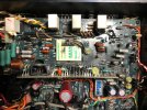
Here's a few pics of the two variations of the Super A Bias Board. Top pic is the Japan Victor version, the other U.S. JVC version.
- Japan version: from 07/1981 (on mini relay), thermistor attached to VC5022 chip
- US version: can't make out the date, thermistor not attached to anything (?!?)
- My version: from 03/1979, has thermistor attached to prehistoric Super-A block
I will post the schematic soon.

Jcandy
New Member
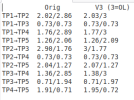
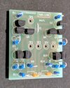
Here is my first prototype of the new Super-A board. It uses BC547 and BC557 transistors to replace 2SC458 and 2SA1029 (as well as the original dual transistors 995/2291). The 5*4=20 possible pin-pin diode voltages match my JVC working version. New transistors have higher gain than the originals but function of the board should have low sensitivity to that.
Attachments

zenith2134
Lunatic Member
Hi,
Fantastic work! These amps are special and deserve a proper servicing.
Fantastic work! These amps are special and deserve a proper servicing.
Jcandy
New Member
Thanks! My intention is to create open-source versions of the TAD-198 (the original board with resistors and transistors circa 1979) and hopefully the TAD-200 (updated board for 1980+)Hi,
Fantastic work! These amps are special and deserve a proper servicing.

ElectTech
Active Member
Congratulations! This is nice and hard work! I compared the reverse engineering you did of the Super-A block (TAD-198), and it looks more like Version #1 of the VC5022 integrated circuit. (I have a JVC A-X1 made in 1980, and I really like how Super-A sounds.) Please inform if your first prototype of the new Super-A board met the specifications (voltage, calibration, etc.) in the JVC service manual of your equipment. Thanks.Thanks! My intention is to create open-source versions of the TAD-198 (the original board with resistors and transistors circa 1979) and hopefully the TAD-200 (updated board for 1980+)


Jcandy
New Member
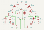
Here's a revised schematic (with updated transistors), PCB layout, and pin-to-pin voltage drop (diode) numbers comparing original to prototype (V3). The numbers are voltage drops between test points with multimeter in diode mode (forward/reverse). Agreement is nearly perfect but the multimeter gives OL for 3V drops because this exceeds the capability of the multimeter. I had put this project hold but will resume soon.