What I have are the TO3 package, MJ15003 & MJ15004 transistors, I pair per channel. Both are in stock at DigiKeyDepending on which type you have, you might want to check that. TO3 package ones are, the later plastic MT200(?) ones aren't.


You are using an out of date browser. It may not display this or other websites correctly.
You should upgrade or use an alternative browser.
You should upgrade or use an alternative browser.
What I have are the TO3 package, MJ15003 & MJ15004 transistors, I pair per channel. So it would be the later version or someone did the mods prior. I downloaded the SM when I bought the unit, but only did a quick scan of the schematics and parts list. Did not think to read further and go through the SBs, of which there are many - probably not a good sign, lol. Many thanks to you and others in this thread, for all the generous advice given.If both channels are doing the same, it does tend to suggest damaged transistors in both final output stages - note, there was an early output stage design, with 6 transistors per channel, and a later version with simplified drivers, so only 4 per channel - you obviously need to check which you have. If the bias pots were both already set fully CW, then you also know someone's been there before... and anything's possible.
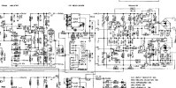
R215 is a known problem (it needs upgrading to 0.5W) - you'll find it in the service bulletins, they're in the hfe SM if you don't already have them.
I'd suggest to have a good review of the full SM & Service bulletins before tearing too far into it, there are a number of potential changes documented in the SB's., and to check your PS voltages are all +/- correct.
H
ThanksDepending on which type you have, you might want to check that. TO3 package ones are, the later plastic MT200(?) ones aren't.
Finally got around to de-soldering the output transistors from the board. Had expected to find at least one shorted, but that was not the case, as my Peak Atlas tester recognized all 4 as the correct PNP and PNP types. The hFE values were very low on 3 of them, 11, 37 and 40 respectively. Planning to replace all 4 with new, along with pertinent SB recommendations from the SMWhat I have are the TO3 package, MJ15003 & MJ15004 transistors, I pair per channel. So it would be the later version or someone did the mods prior. I downloaded the SM when I bought the unit, but only did a quick scan of the schematics and parts list. Did not think to read further and go through the SBs, of which there are many - probably not a good sign, lol. Many thanks to you and others in this thread, for all the generous advice given.

Did the multimeter diode tests prior and the readings were between 0.45 and 0.58v drop or OL for NPN and PNP for the related test connections. The voltage drop readings are low, but within acceptable range. Never was too fond of testing with a multimeter, which is why I got the Peak Atlas unit. Any other recommendation? I was sure at least one output transistor would be at fault, but based on my testing this may not be the case and I may need to dig a bit deeper.The hFE values are probably not very accurate with the Peak Atlas anyway - the test current will be too low for TO-3 output transistors
Tha
Thank you for the quick reply. I think I will leave this for now, noodle on it and get back into it next week. Enjoy your weekendI'd believe the diode tests, and the Peak Atlas, just not for hFE values on the outputs. The output transistors are spec'd for much higher currents that the usual testers supply, e.g., the MJ003 hFE spec. for example is 25 - 150, but at Ic=5A
My output transistors for Q623, Q624, Q625 & Q626 arrived today. I have the existing ones disconnected from the board, but still mounted to the heat sink. Thought that prior to the swap out, I would test the voltage levels, from the board connections, for any inconsistencies. For the PNP (Q625 & Q626) I get +1.35, -44 & -44 VDC at the Emitter, Collector & Base connections respectively. For the NPN (Q623 & Q624) I get +1.35, +43.6 & -44 VDC at the Emitter, Collector & Base connections respectively. So all appear to be consistent, and except for the low hFE values on 3 of the output transistors as discussed prior and concluded that may not be accurate, I really don't see anything dramatic. Any thoughts?Tha
Thank you for the quick reply. I think I will leave this for now, noodle on it and get back into it next week. Enjoy your weekend
Yes that is correct, with dim bulb tester connected to PS, at volume at about 20%, not that it probably makes a difference.. Just to clarify, to me "driver" means the output transistors, which in my case are disconnected. Are you referring, to one or more of the downstream transistors, that are "driving" the output stage? ThanksWith -44V (I assume using a bulb/current limiter ?) on all 4 output transistor base connections, I'd be checking the drivers, esp. on the pnp side.
Sorry for the delay in my updates, but other matters to attend to. Based on measurements taken and reported earlier, the problem(s) that I have are common to both channels.
So looking at the PS circuit in more detail there are considerable heat traces in the area encompassing C808 and C816. This is giving off a lot of heat with outputs still disconnected and obviously no load. Several caps look fried and probably nearby transistors as well. Needless to say some desoldering and testing ahead.
So looking at the PS circuit in more detail there are considerable heat traces in the area encompassing C808 and C816. This is giving off a lot of heat with outputs still disconnected and obviously no load. Several caps look fried and probably nearby transistors as well. Needless to say some desoldering and testing ahead.
Attachments

StimpyWan
Addicted Member
Pardon my ignorance, as I'm not a bench tech, and I'm going on distant memory, but I had a 3140 that suddenly died. I took it into a coworker tech. He found that the peak display meters had caused my faults. That the output signal routed through them, and a component failure there, had killed the output signal. Repairing the peak meter circuitry repaired the amp. Vague, but I hope this helps...!
Thank you for the advice. My display LEDs partially light up. The power meters I cannot verify, as I have yet to get that far. There are a host of issues with this unit, but I think the key is my last update, referencing the power supply related observations. Will update, once I get that far.Pardon my ignorance, as I'm not a bench tech, and I'm going on distant memory, but I had a 3140 that suddenly died. I took it into a coworker tech. He found that the peak display meters had caused my faults. That the output signal routed through them, and a component failure there, had killed the output signal. Repairing the peak meter circuitry repaired the amp. Vague, but I hope this helps...!
Some more parts came in today and I completed what I would consider as critical revisions covering the power amplification section and including all 4 output transistors. Able to adjust DC off-set and idle current, without the runaway condition as before, but I am still concerned that there is too much current draw, as I am getting a steady orange glow, from my dim bulb tester, with no input connected and no output to speakers. Will test with signal generator and scope next.The 'drivers' are the transistors immediately before the 'outputs' - they drive the output transistors. I don't know what your amp schematic / numbering is, but it'll be the ones directly connected to the bases of the outputs.
Attachments

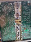
I believe we have success. Using the Aux input with my phone connected, I am getting consistent output voltages for both channels on the speaker terminals and sound on the headphones. Yet to connect speakers, but this should not be a problem as I am not seeing the run away condition as before. LED power meters are working properly also. Still some clean up with caps (glue and signs of corrosion) along with replacing the adjustment potsSome more parts came in today and I completed what I would consider as critical revisions covering the power amplification section and including all 4 output transistors. Able to adjust DC off-set and idle current, without the runaway condition as before, but I am still concerned that there is too much current draw, as I am getting a steady orange glow, from my dim bulb tester, with no input connected and no output to speakers. Will test with signal generator and scope next.
One more observation. With Aux input on both channels, speakers connected, but volume at 0%, I get a baseline current draw of 300mA. That can't be right and I still have a short somewhere in the system. Without the dim bulb tester I would probably be blowing fuses or worse.Spoke too soon. With dim bulb tester inline, both channels play, with speakers connected, but I am seeing 0.5A supply current draw @115VAC at about 30% volume. That works out to 60W. This amp is rated for 40W, so I should have much more headroom.