• The move to the new server is done. There are some software and database maintenance updates in process. This has us passing the hat around to help out. We appreciate any donations. Seriously, even a dollar helps. The payment page may be found here - https://www.audiokarma.org/support.html

Pioneer SX-535 with blown fuses F7 and F8

prenex

New Member
Hi, greetings from a beginner in the Hi-Fi world. I’m not unfamiliar with electronics repair and working with a soldering iron, but I’m still an amateur and mostly involved with retro computers. I recently bought a Pioneer SX-535 that wasn’t producing sound from the right channel. I opened it up and after a visual inspection, I found a cracked transistor (Q10 on the AWH-035) and a burnt resistor (R-28).

I ordered replacement transistors for the entire AWH-035 from AliExpress and replaced all of them on the channel with the cracked transistor, as well as Q1 and Q3 on the other side. I also replaced Q11, Q12, Q13, and Q14, so on both channels.

Before installing the components, I checked them with an LCR-T4 component tester to make sure of the polarity so I could place them correctly on the board. However, Q13 and Q14 (KSB596YTU) turned out to be reprinted fakes — they weren’t PNP transistors but NPN ones. I hadn’t paid attention to that, even though I had the component tester, I only checked the polarity.

After the first power-up, fuses F7 and F8 blew. Later, I ordered and installed new Q13 and Q14 — this time I checked them, and they really are KSB596YTU PNP transistors — but F7 and F8 blew again. I’m posting here the voltages I measured on the AWR-067 pins.


Any help is welcome…
 
Register to hide this ad
PinAWR-067 (Power Supply Board)
121 V AC
2–0.046 V DC
38 V AC
48 V AC
521 V AC
60.036 V DC
736 V AC
836 V AC
90 V
10–43 V DC
110 V
1213.4 V DC
1313.4 V DC
1413.4 V DC
150 V
1630 V
1730 V
 
Last edited:
+1 on checking the output transistors. If you find a bad one (bet you will) be sure to test its emitter resistor.

I think you have proven a point that is mentioned over and over again. Only buy your parts from people/distributors/re-sellers with proven track records for selling legitimate parts.

In the states the big suppliers would be DigiKey, Mouser, Newark and a handful of smaller dealers.

Maybe, you will find NOS out there, and there are some legitimate dealers that specialize in surplus NOS or hard to find parts.

You may also find used "pulls", typically on the auction sites.

I personally would not trust the rest of the transistors you got from AliExpress.

Smart move to test the part for pinout, some subs are not the same.

The power supply voltages all look good except the main + and - voltage for the power amplifier, which is the supply with the blown fuses.
 
The amp section of this receiver is easy to perform the "lazy method" on. This is testing the amp without output transistors. Usually you need to make a connection to restore the feedback path but in this design that is not necessary. Remove the output transistors from the bad channel and test the voltage on the output (no load, should be zero). Also check the voltage between the emitters of Q7 & 8. Should be as per schematic.

You could also use a DBT but they sometimes upset the working conditions of the amp. But it will save your fuses.
 
Thank you all for the quick responses.… here’s what I did: I double-checked the polarity of the transistors I had previously replaced and found an error — Q8 was installed incorrectly, which I have now corrected. After that, I checked the voltages on the transistors on both sides, and everything matched correctly.

Then I soldered in new Q11, Q12, Q13, and Q14. I put in new fuses F7 and F8. I powered on the receiver, and everything looked fine at first, but after a few seconds (~5 seconds), fuse F8 blew again.

I removed Q11, Q12, Q13, and Q14 again. Q11 and Q13 are fine. Q12 is completely shorted, and Q14 has now effectively turned into two resistors.

Progress has been made — fuse F7 no longer blows — but the question remains: what is so relentlessly destroying Q12, Q14, and fuse F8?
 
Do the "lazy method". You can do it now.

Fun fact: it's called "lazy" because I am a lazy engineer and don't want to replace transistors that have blown a second time. The "lazy method" prevents that.
 
leave q12 q14 out until the rest is fixed properly or you will soon be spending huge amounts of money on expensive transistors .
 
As @PE9ZZ mentioned:
You could also use a DBT but they sometimes upset the working conditions of the amp. But it will save your fuses.
DBT might have saved the fuse and the output transistor. If you don't know what a DBT is there are plenty of threads and on-line videos about how to make and use one.

Were the outputs from AliExpress as well? It may have popped because it was a fake.
 
Do not buy parts on Aliexpress. Be very careful buying parts on ebay. In fact, unless you really know what you're looking at, don't buy parts on ebay either.
 
2SC789a —> KSD526Y
2SA489a —> KSB596Y
these you should be able to find genuine . i believe they are good subs
edit ... whoops sorry i didn't realise they are now obsolete .
 
OK, a small update… I desoldered Q11–Q14 and replaced Q6, Q8, and Q10 again. I built a DBT (dim bulb tester), installed a new F8 fuse, powered on the unit, and started measuring voltages on both channels (the working and the faulty one).

More or less everything is the same except the base of Q9 is -1.22 V and the base of Q10 is -1.44 V. Q5’s emitter is -1.22 V, and on Q7 it’s -1.44 V — and what is, as I understand, most important: the base of Q7 is +1.22 V and the base of Q8 is +1.2 V, whereas they should be -1.2 V.

Then I moved the transistors from one channel to the other and got the same results again, which means the problem isn’t in the transistors.

I also resoldered all the points on the AWH-035 to eliminate any cold solder joints.
 
OK, a small update… I desoldered Q11–Q14 and replaced Q6, Q8, and Q10 again. I built a DBT (dim bulb tester), installed a new F8 fuse, powered on the unit, and started measuring voltages on both channels (the working and the faulty one).

More or less everything is the same except the base of Q9 is -1.22 V and the base of Q10 is -1.44 V. Q5’s emitter is -1.22 V, and on Q7 it’s -1.44 V — and what is, as I understand, most important: the base of Q7 is +1.22 V and the base of Q8 is +1.2 V, whereas they should be -1.2 V.

Then I moved the transistors from one channel to the other and got the same results again, which means the problem isn’t in the transistors.

I also resoldered all the points on the AWH-035 to eliminate any cold solder joints.
I appreciate the "Gung Ho" attitude but caution you about swapping parts back and forth.

Several reasons for that caution. All of of these old circuit boards won't take a lot of re-work well, even if you are careful. You can risk lifted or cracked traces and pads.

Putting all known good transistors in a circuit that was not working risks making one or more of them into bad transistors. The bad channel could have a shorted cap, a shorted trace, a new solder bridge that you created by moving parts, open resistors and other "stuff". All those things could lead to two not working channels in the end. :yikes:

IMO it is best to leave a working channel alone and use it as a reference for voltages and resistances.
 
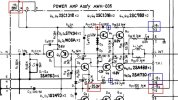
Let's confirm we have good power supply voltages where we need them.

The blue box power supplies (B1) are for the output transistors and the driver transistors.
Check the incoming + and - voltages at Pins 13 and 16 I will assume they are present since one channel is working, but best to check.
Then check the collectors of the drivers.

Now look at the red box (B2) voltages which power the rest (front end) amplifier circuit.
Check the incoming + and - voltages at 12 and 14. I will assume it is there since one channel works, but best to check.
Then check the other two red points.

sx535pa.jpg
 
Last edited:
If you are curious about how this amp works @markthefixer explains it better than I can here:

 
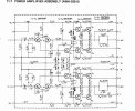
This becomes confusing because we don't have a full schematic. What transistors QX? are in the bad channel?
Or put another way on the schematic I posted above are the transistors in the full circuit in the good or bad channel?

On the bad channel what are the collector voltages of what is shown as Q7 and Q9 in the schematic.


L R
Q1=Q2
Q3=Q4
Q5=Q6
Q7=Q8
Q9=Q10
Q11=Q12
Q13=Q14
 
All even numbers are on the right channel which is faulty.

Q6 collector = -1.44V

Q10 collector = -26.2V
 
Last edited:
Back
Top Bottom