

You are using an out of date browser. It may not display this or other websites correctly.
You should upgrade or use an alternative browser.
You should upgrade or use an alternative browser.
Sansui B-2301L / Sansui C-2301 restoration
- Thread starter Bumpalump
- Start date


JOMARK911
Super Member
So i thought to remind you about the adjustment page of c2301 .Yes i have, remind me in monday, so Ill upload that page

@JOMARK911
Let me try to explain it in simple terms - there are basically two ways of adjusting the offset:
version ( A ) -> trimming the "equivalent source resistors" of the JFET's LTP
version ( B ) -> connecting the CCS coming from V- directly to JFET's LTP (no source resistors) and putting a trimmer on the drain side, on the V+. The other side of the LTP has a fixed resistor in the drain, like usual.
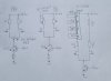
For some reason, in case of C-2301 and C-2302 Sansui opted for version (B). But, instead of putting a trimmer (variable resistor) they put 4 resistors in series, each of them being (or not) bypassed with the 4 switches from SW1 - depending on each switch position. This SW1 arrangement behaves similar to a stepped attenuator. Based on the switches position, you obtain the values from the above tables. ON = switch closed (R shorted), OFF = switch open (R in circuit). The simplified schematic is below.
Depending on the double JFET matching, you are basically trying to "compensate" that 75R from the right side of the LTP with some combination of resistors from the left side, so that LTP is better balanced and DC offset is minimized.
Hope this clears it up.
Regards
Let me try to explain it in simple terms - there are basically two ways of adjusting the offset:
version ( A ) -> trimming the "equivalent source resistors" of the JFET's LTP
version ( B ) -> connecting the CCS coming from V- directly to JFET's LTP (no source resistors) and putting a trimmer on the drain side, on the V+. The other side of the LTP has a fixed resistor in the drain, like usual.
For some reason, in case of C-2301 and C-2302 Sansui opted for version (B). But, instead of putting a trimmer (variable resistor) they put 4 resistors in series, each of them being (or not) bypassed with the 4 switches from SW1 - depending on each switch position. This SW1 arrangement behaves similar to a stepped attenuator. Based on the switches position, you obtain the values from the above tables. ON = switch closed (R shorted), OFF = switch open (R in circuit). The simplified schematic is below.
Depending on the double JFET matching, you are basically trying to "compensate" that 75R from the right side of the LTP with some combination of resistors from the left side, so that LTP is better balanced and DC offset is minimized.
Hope this clears it up.
Regards