Preface:
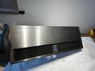
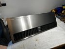
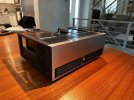
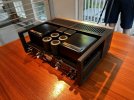
Hey everyone! It's been a while since I've posted here or on YouTube, so I wanted to share an update about a project I started back in June. Life has been pretty hectic with work and everything else, leaving me little time for any repair or restoration projects. However, I did carve out some time to fully restore a friend's Sony TA-N7B, which was a fun challenge.
To tackle this restoration, I had to head over to my friend's place and set up my workspace there. Over the course of a month or two, I made several trips back and forth to get everything sorted out and complete the job. It was a bit of a journey, but totally worth it to see (and hear) the final result!
To provide some background, my friend has been rolling through amplifiers left and right, trying to find the best mate to his B&W 801 S3 speakers. I had loaned my restored Sony TAN-5550 to him for use, and we were thoroughly impressed with the overall synergy of the setup, although we found the bass response to be somewhat lacking. This would not pose a problem with smaller speakers; however, the 801s require significant power and finesse from an amplifier in order to really open up. I casually suggested that the N7B could potentially offer an ideal solution, given its unique hybrid BJT and VFET output stage, and before I knew it, he had one delivered to his doorstep!
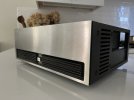
The example he chose was generally in decent shape. There were a few small nicks on the top edge of the faceplate, and the transformers had been repainted by the last owner rather haphazardly. Speaking of which, the previous owner had also done quite a bit of questionable work inside while swapping out the death diodes and installing new, higher-spec BJT output devices. We'll dive into that more later. The amplifier was inspected and briefly tested in his system with no obvious faults. After testing, I got the amplifier on the bench and began work.
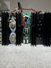
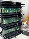
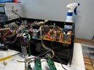
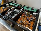
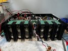
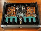
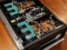
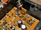
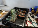
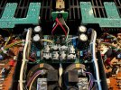
As you can see from the preliminary photos below, the previous guy hadn't put much care or attention into the work he did. There was lots of burned flux residue on the board where he was prodding around. Not to mention all of the dust and dirt on the boards, as well as a bunch of cracked solder joints he had overlooked. It appears that on top of removing and replacing the double diode packages, he had also removed the relays in order to sand the contacts down. This didn't matter, as I was planning to swap the original relays out with new anyways.
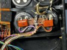
Also note the thorough use of wire-wrap terminals in this amp. I am generally not against wire wrap terminals when they are of high quality and used in moderation. In the N7B's case though, Sony opted to use very cheap terminal assemblies that melt when even the slightest amount of heat is applied during the unsoldering and soldering process. Pair this with the sheer amount of them in the amp, and the lack of service loop in the wiring, it makes for a very difficult time for me to work with them. The terminals had to go, so after much deliberation with my accomplice, we decided that the next best thing was to use high quality gold plated cup terminals. This allows for the wires to be unsoldered and soldered from the top side of the board, if and when board removal is necessary. No more bending the board around at risk of stress cracking the wires, like what happens with wire wrap terminals.


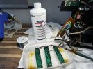
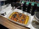
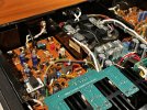
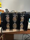
Seen here is another clear case of the lack of effort and care that was put into the previous work done to this amplifier. I know thermal paste is messy, but it doesn’t take much to clean up after yourself!
Left Channel "Power Amp" Board:
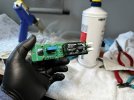
I started on the left channel amplifier PCB, as this was the easiest board to remove. I completed a thorough inspection of the components, as well as the condition of the board. Even though the previous soldering was a mess, I was able to determine that the circuit trace integrity was okay. I began by replacing all electrolytic and film capacitors on the board. Afterwards, I removed and replaced all diodes and transistors on the board. While I was at it, I also replaced the dual 1N4148s in series that were installed previously, in place of the notorious death diodes. I wasn't sure of the quality of parts that were used here, and I wanted to be sure that they wouldn't cause any trouble. 1N4148s cost pennies, but peace of mind is priceless! On this note, some of the things to look for if you are working on a TA-N7B are the failing fusible resistors and dual diodes. Another hidden gremlin is the foam that is used under the amplifier circuit boards by each of the relays. When this foam breaks down, it becomes corrosive and can damage the traces on the circuit boards! Such was the case with this unit. Luckily there isn't any corrosive glue used in the N7B that I've seen, so you should be safe from that thankfully.
Also replaced were the trimmers for bias and offset. The original single-turn offset potentiometer was replaced with a high quality multi-turn trimmer for more precise offset adjustment ability. Also done was the installation of a 6-pin DIP socket for the input differential package, as well as the replacement of the fusible resistors and a few key resistors in the feedback loop in favor of high precision metal film parts. Components from companies like Nichicon, United Chemi-Con, Vishay / Dale, Onsemi, and Toshiba are used on this board and all others in this restoration. No-name, substandard parts have no place in amplifiers of this caliber.
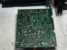
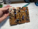
Shown below is the semi-finished product of the board, sans a few components such as the replacement output relay. The board really cleaned up well, and I was very happy with how it turned out, especially the solder side!

Amplifier "Connection" Boards:
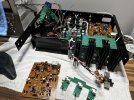
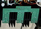
Upon inspection of the amplifier, the output connection boards were found to be damaged due to careless removal and installation of the BJT output devices. The traces that supported the legs of the BJTs were mangled. The boards could have been saved, but due to the critical nature of this area, it was decided that the replacement of the boards would be the best course of action. My friend measured the original boards and replicated a new set that I then populated with new components, including the new D45H11/D44H11 BJT output devices and new KOA Speer emitter resistors.

Hey everyone! It's been a while since I've posted here or on YouTube, so I wanted to share an update about a project I started back in June. Life has been pretty hectic with work and everything else, leaving me little time for any repair or restoration projects. However, I did carve out some time to fully restore a friend's Sony TA-N7B, which was a fun challenge.
To tackle this restoration, I had to head over to my friend's place and set up my workspace there. Over the course of a month or two, I made several trips back and forth to get everything sorted out and complete the job. It was a bit of a journey, but totally worth it to see (and hear) the final result!
To provide some background, my friend has been rolling through amplifiers left and right, trying to find the best mate to his B&W 801 S3 speakers. I had loaned my restored Sony TAN-5550 to him for use, and we were thoroughly impressed with the overall synergy of the setup, although we found the bass response to be somewhat lacking. This would not pose a problem with smaller speakers; however, the 801s require significant power and finesse from an amplifier in order to really open up. I casually suggested that the N7B could potentially offer an ideal solution, given its unique hybrid BJT and VFET output stage, and before I knew it, he had one delivered to his doorstep!
The example he chose was generally in decent shape. There were a few small nicks on the top edge of the faceplate, and the transformers had been repainted by the last owner rather haphazardly. Speaking of which, the previous owner had also done quite a bit of questionable work inside while swapping out the death diodes and installing new, higher-spec BJT output devices. We'll dive into that more later. The amplifier was inspected and briefly tested in his system with no obvious faults. After testing, I got the amplifier on the bench and began work.
As you can see from the preliminary photos below, the previous guy hadn't put much care or attention into the work he did. There was lots of burned flux residue on the board where he was prodding around. Not to mention all of the dust and dirt on the boards, as well as a bunch of cracked solder joints he had overlooked. It appears that on top of removing and replacing the double diode packages, he had also removed the relays in order to sand the contacts down. This didn't matter, as I was planning to swap the original relays out with new anyways.
Also note the thorough use of wire-wrap terminals in this amp. I am generally not against wire wrap terminals when they are of high quality and used in moderation. In the N7B's case though, Sony opted to use very cheap terminal assemblies that melt when even the slightest amount of heat is applied during the unsoldering and soldering process. Pair this with the sheer amount of them in the amp, and the lack of service loop in the wiring, it makes for a very difficult time for me to work with them. The terminals had to go, so after much deliberation with my accomplice, we decided that the next best thing was to use high quality gold plated cup terminals. This allows for the wires to be unsoldered and soldered from the top side of the board, if and when board removal is necessary. No more bending the board around at risk of stress cracking the wires, like what happens with wire wrap terminals.
Seen here is another clear case of the lack of effort and care that was put into the previous work done to this amplifier. I know thermal paste is messy, but it doesn’t take much to clean up after yourself!
Left Channel "Power Amp" Board:
I started on the left channel amplifier PCB, as this was the easiest board to remove. I completed a thorough inspection of the components, as well as the condition of the board. Even though the previous soldering was a mess, I was able to determine that the circuit trace integrity was okay. I began by replacing all electrolytic and film capacitors on the board. Afterwards, I removed and replaced all diodes and transistors on the board. While I was at it, I also replaced the dual 1N4148s in series that were installed previously, in place of the notorious death diodes. I wasn't sure of the quality of parts that were used here, and I wanted to be sure that they wouldn't cause any trouble. 1N4148s cost pennies, but peace of mind is priceless! On this note, some of the things to look for if you are working on a TA-N7B are the failing fusible resistors and dual diodes. Another hidden gremlin is the foam that is used under the amplifier circuit boards by each of the relays. When this foam breaks down, it becomes corrosive and can damage the traces on the circuit boards! Such was the case with this unit. Luckily there isn't any corrosive glue used in the N7B that I've seen, so you should be safe from that thankfully.
Also replaced were the trimmers for bias and offset. The original single-turn offset potentiometer was replaced with a high quality multi-turn trimmer for more precise offset adjustment ability. Also done was the installation of a 6-pin DIP socket for the input differential package, as well as the replacement of the fusible resistors and a few key resistors in the feedback loop in favor of high precision metal film parts. Components from companies like Nichicon, United Chemi-Con, Vishay / Dale, Onsemi, and Toshiba are used on this board and all others in this restoration. No-name, substandard parts have no place in amplifiers of this caliber.
Shown below is the semi-finished product of the board, sans a few components such as the replacement output relay. The board really cleaned up well, and I was very happy with how it turned out, especially the solder side!
Amplifier "Connection" Boards:
Upon inspection of the amplifier, the output connection boards were found to be damaged due to careless removal and installation of the BJT output devices. The traces that supported the legs of the BJTs were mangled. The boards could have been saved, but due to the critical nature of this area, it was decided that the replacement of the boards would be the best course of action. My friend measured the original boards and replicated a new set that I then populated with new components, including the new D45H11/D44H11 BJT output devices and new KOA Speer emitter resistors.
Last edited:
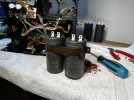


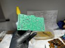
 After I got the board, I did the grunt work of populating and installing it. It turned out great!