MartinAudio
Young Collector
Some time ago, a friend of mine inquired about purchasing a VFET amplifier, and was veering towards a Sony TA-N7b. However due to both their expense and rarity, he decided to go with the more common and easily servicable TAN-5550 model. I've worked on a few of these at this point and know the ropes on what they need, some improvements here and there, and making them reliable. Replacing the "death diodes", noisy black leg TO92 transistors and obsolete package driver transistors, the often poorly contacting speaker relay, and more were all on the radar for this one.
After some time he pulled the trigger on one and had it sent straight to me for a full top down restoration. When it arrived I knew it was going to be interesting for sure! Somebody at some point must have smacked one of the volume pots hard, enough to shear off the shaft and scratch up the faceplate. Overall this unit was in good condition, especially the fake wood side panels that like to delaminate and fall apart over time.
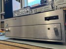
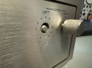
But on the side of good news, the internals were entirely original! No hack work, poor soldering, or modifications could be seen anywhere. A perfect restoration candidate once the cosmetics were figured out on replacing that potentiometer and knob assembly. More on that later.
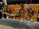
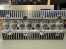
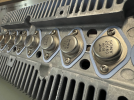
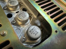
After reviewing the ad, it appeared the seller powered the unit on and described it as working, and sure enough the amplifier did in fact work upon powering up. The left channel however was intermittently cutting out, and the sound was dull and murky, not something that should be the case for a TAN-5550, so this unit was definitely tired and needing a proper top down restoration to get it back into performing beautifully. Upon taking off the convienent mesh cover plate, we can see a full compliment of original Sony branded 2SK60 and 2SJ18's! It appears that someone poorly attempted to redo the thermal paste, but used about 3x the necessary amount, and smeared it everywhere. That will all have to be cleaned up and new silicon pads will be put in their place.
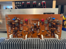
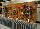
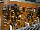
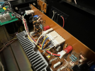
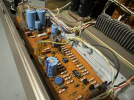
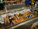
Let's first tackle what Sony calls the Class A board in their service manual. This is a combination board containing the speaker protection relay, a +/- 60v regulated power supply, and the amplifier front end circuitry using two Sony 2SK58 dual JFETs in a differential pair. This is also where your DC offset adjustments are made via the top blue trimmers.
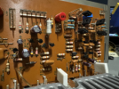
As discussed before, we were experiencing channel dropoff and this right here was our culprit. This isn't the first 5550 I've seen with what appears to be a defective relay. If you look closely, you can see the contact plates which are meant to be straight are all crooked and misaligned causing poor contact.
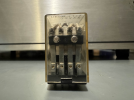
After replacing that with a brand new Omron relay, our dropoff problem went away! But that isn't the only thing we need to do, we are just getting started. In a short order, here is a list of things done to the Class A board.
The next job to tackle is the power supply/filter capacitor assembly. This board simply attaches to the existing filter capacitor screw terminals via 4 copper plates attached to the PCB. This board provides your +/- 53vdc for your amplifier assembly, along with a dropping resistor to provide voltage to the green power indicator bulb.
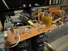
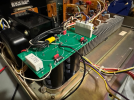
Besides being caked in dust, this is a bit of trickier issue to deal with, as the filter capacitors are no longer available in this size profile. The diameter of the capacitor actually expands where it meets the bracket, and there just isn't anything like this made by anyone. The .5" screw terminal capacitors on their own are already relatively uncommon, so these are NLA at this point. Because the PCB is lifted and supported by these capacitors, it is necessary to choose the right ones and I was not able to find anything from my suppliers. So a bit of development later, and I designed a new power supply PCB to replace the original, one that can accomodate brand new modern capacitors that are the right diameter.
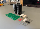
New board assembled.
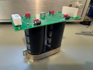
Vs the original.
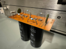
This new board allows multiple improvements to be made over the original, such as increasing the power rating of the power indicator dropping resistor to a 5 watt ceramic, as it can get very very hot and cook the resistor over time. The original part was only rated for 3 watts, so this should last much longer. The new board also incorporates provisions for modern fast diodes, along with more optimally placed WIMA capacitors to filter out any switching noise. Instead of using the cheap wire wrap terminals like they did originally, I am using machined brass terminals made by Mill-Max. The ground terminal originally was attached to one of the capacitor screws, but now it is attached to its own dedicated ground terminal on the PCB.
Next up I'll be tackling installation of the power supply board, rebuilding the power amplifier board, dealing with the cosmetics, and more.
After some time he pulled the trigger on one and had it sent straight to me for a full top down restoration. When it arrived I knew it was going to be interesting for sure! Somebody at some point must have smacked one of the volume pots hard, enough to shear off the shaft and scratch up the faceplate. Overall this unit was in good condition, especially the fake wood side panels that like to delaminate and fall apart over time.
But on the side of good news, the internals were entirely original! No hack work, poor soldering, or modifications could be seen anywhere. A perfect restoration candidate once the cosmetics were figured out on replacing that potentiometer and knob assembly. More on that later.
After reviewing the ad, it appeared the seller powered the unit on and described it as working, and sure enough the amplifier did in fact work upon powering up. The left channel however was intermittently cutting out, and the sound was dull and murky, not something that should be the case for a TAN-5550, so this unit was definitely tired and needing a proper top down restoration to get it back into performing beautifully. Upon taking off the convienent mesh cover plate, we can see a full compliment of original Sony branded 2SK60 and 2SJ18's! It appears that someone poorly attempted to redo the thermal paste, but used about 3x the necessary amount, and smeared it everywhere. That will all have to be cleaned up and new silicon pads will be put in their place.
Let's first tackle what Sony calls the Class A board in their service manual. This is a combination board containing the speaker protection relay, a +/- 60v regulated power supply, and the amplifier front end circuitry using two Sony 2SK58 dual JFETs in a differential pair. This is also where your DC offset adjustments are made via the top blue trimmers.
As discussed before, we were experiencing channel dropoff and this right here was our culprit. This isn't the first 5550 I've seen with what appears to be a defective relay. If you look closely, you can see the contact plates which are meant to be straight are all crooked and misaligned causing poor contact.
After replacing that with a brand new Omron relay, our dropoff problem went away! But that isn't the only thing we need to do, we are just getting started. In a short order, here is a list of things done to the Class A board.
- Replace all electrolytic capacitors with Nichicon low impedance 105C rated parts.
- Replace the two trimmers with Bourns 3386-P series parts.
- Replace the infamous VD-1221 "death diode" with two 1N4148's in series.
- Replace the speaker protection relay with an Omron MY4-02-DC24V part.
- Replace all the transistors with equivalent, appropritately chosen On-Semi transistors.
The next job to tackle is the power supply/filter capacitor assembly. This board simply attaches to the existing filter capacitor screw terminals via 4 copper plates attached to the PCB. This board provides your +/- 53vdc for your amplifier assembly, along with a dropping resistor to provide voltage to the green power indicator bulb.
Besides being caked in dust, this is a bit of trickier issue to deal with, as the filter capacitors are no longer available in this size profile. The diameter of the capacitor actually expands where it meets the bracket, and there just isn't anything like this made by anyone. The .5" screw terminal capacitors on their own are already relatively uncommon, so these are NLA at this point. Because the PCB is lifted and supported by these capacitors, it is necessary to choose the right ones and I was not able to find anything from my suppliers. So a bit of development later, and I designed a new power supply PCB to replace the original, one that can accomodate brand new modern capacitors that are the right diameter.
New board assembled.
Vs the original.
This new board allows multiple improvements to be made over the original, such as increasing the power rating of the power indicator dropping resistor to a 5 watt ceramic, as it can get very very hot and cook the resistor over time. The original part was only rated for 3 watts, so this should last much longer. The new board also incorporates provisions for modern fast diodes, along with more optimally placed WIMA capacitors to filter out any switching noise. Instead of using the cheap wire wrap terminals like they did originally, I am using machined brass terminals made by Mill-Max. The ground terminal originally was attached to one of the capacitor screws, but now it is attached to its own dedicated ground terminal on the PCB.
Next up I'll be tackling installation of the power supply board, rebuilding the power amplifier board, dealing with the cosmetics, and more.