• The move to the new server is done. There are some software and database maintenance updates in process. This has us passing the hat around to help out. We appreciate any donations. Seriously, even a dollar helps. The payment page may be found here - https://www.audiokarma.org/support.html

Unable to Lower DC Offset

GabrielS

Active Member
Been working on my Luxman L-100 integrated amp that powers on with relay clicks. Am able to adjust bias to the specified 60ma but the dc offset remains at -3.6v regardless of trimmer pot adjustment. Been working on this for months to no avail. Any help appreciated in tracking down the possible causes and remedies.
 
Register to hide this ad
Another vote for looking at the differential pair (Q401,2) consider replacing with a hfe matched pair.

Very odd that offset does not respond to VR401 adjustment, maybe faulty VR??? Also check R402(100k) is still in the ballpark, it will be. Doubtful it would be a bad solder connection, ie, open circuit somewhere.

Confirm no response to VR401 adj.
Check VR401, R402 then replace Q401,2
 
consider replacing with a hfe matched pair
I have to downvote. A large offset like this is not caused by the input stage. You will find that it also clips at different levels because the current sources Q405 or Q407 are malfunctioning. Prolly. Check the two double diodes D401 & D402. Check for 0.7 V (ish) across R410 and R411. Check for identical voltages across R405 and R406. If borked D401/2 can be replaced with two 1N4148 in series.
 
Thank you for all your responses and contributions. I'll print this then follow through with the info you've given. ☺️
 
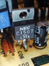
After careful examination of left and right channel boards of PB649. I found Q406 (C1507) of the left channel was incorrectly placed on the board having the emitter going to where the collector would be and reoriented it to the proper position. This might be the cause of the dc offset issue. But before assembling everything and powering up, I found something else of concern on both left and right boards. Q405 (C536) pins (B, C, E) measures differently once applied to the circuit board. Instead of B, C, E measured out of circuit, it now measures C, E, B when mounted. They were mounted correctly according to the nomenclature printed on the circuit boards. Could this be an error of pin orientation printed on the boards or is this caused by the interaction of other components on the board causing this? I'm leaning towards the transistor is correctly mounted, but the reading is now being affected by the interaction of other components. Thoughts please!
 
I have to downvote. A large offset like this is not caused by the input stage. You will find that it also clips at different levels because the current sources Q405 or Q407 are malfunctioning. Prolly. Check the two double diodes D401 & D402. Check for 0.7 V (ish) across R410 and R411. Check for identical voltages across R405 and R406. If borked D401/2 can be replaced with two 1N4148 in series.
After careful examination of left and right channel boards of PB649. I found Q406 (C1507) of the left channel was incorrectly placed on the board having the emitter going to where the collector would be and reoriented it to the proper position. This might be the cause of the dc offset issue. But before assembling everything and powering up, I found something else of concern on both left and right boards. Q405 (C536) pins (B, C, E) measures differently once applied to the circuit board. Instead of B, C, E measured out of circuit, it now measures C, E, B when mounted. They were mounted correctly according to the nomenclature printed on the circuit boards. Could this be an error of pin orientation printed on the boards or is this caused by the interaction of other components on the board causing this? I'm leaning towards the transistor is correctly mounted, but the reading is now being affected by the interaction of other components. Thoughts please!
 

Attachments

  • PB649 - Q406 - C1537 - Left Channel Pin Orientation.JPG
    PB649 - Q406 - C1537 - Left Channel Pin Orientation.JPG
    109.8 KB · Views: 23
  • PB649 - Q406 - C1537 - Right Channel Pin Orientation.JPG
    PB649 - Q406 - C1537 - Right Channel Pin Orientation.JPG
    108.8 KB · Views: 21
  • PB649 - Q405 - B536- Left and Right Channel Pin Orientation.JPG
    PB649 - Q405 - B536- Left and Right Channel Pin Orientation.JPG
    77.4 KB · Views: 24
  • PB649  Left and Right Boards.JPG
    PB649 Left and Right Boards.JPG
    110.1 KB · Views: 27
In circuit testing does save time however you need to look at alternate paths and their impact, eg, testing Q406 e(red) c(blk) there is a path from Q406e-Q421b-Q421c-Q406c giving one diode volt drop instead of expected OL, then it comes down to the tester SW which says WTF... BS in BS out.
 
I have an L-100 open right now that I have been working on for over a year. Last night I FINALLY got it to come out of protect and pass a sine wave all the way to the speaker outputs. If I can help with pictures or checking voltages etc let me know, I feel like I know this thing inside out - not saying I understand every single thing about it but I have troubleshot a lot of different problems with this thing. The transistor I had the most problem with on the 649 board and had to replace (more than once) was Q08. The other thing I felt that helped was to remove 649 from the amplifier assembly (board 635) so that the two connectors (C01aM-C04dM, C05aM-C08dM) are not plugged in. Then you can measure the values on these and compare between the left and right channels. The input to the amplifier assembly is the C02b and C06b readings; that way you can see if the problem is with the 649 board or if it is further down stream. Also allows to make sure the power supply to the output transistors is the same - C03cM, C04dM, C07cM, C08cM - off the top of my head I think it was about 66V. C01aM and C05aM is the output of the amplifier modules going to C15M and C16M.

Also I feel like I should put this somewhere in the L-100 threads because it caused me a lot of grief and I haven't seen it mentioned anywhere else. I never noticed the little metal tabs on the metal holder for the equalizer board 636. At one point, I had inserted it with the traces/pads touching one of them and causing a short or something but only sporadically that would take it in and out of protect for seemingly no good reason. I went around in circles forever until I found it. That took me way too long to find and correct.
I have found the L-100 to be one of the more difficult and frustrating amplifiers I have tried to tackle, but I have learned a lot along the way with it.
 
I have an L-100 open right now that I have been working on for over a year. Last night I FINALLY got it to come out of protect and pass a sine wave all the way to the speaker outputs. If I can help with pictures or checking voltages etc let me know, I feel like I know this thing inside out - not saying I understand every single thing about it but I have troubleshot a lot of different problems with this thing. The transistor I had the most problem with on the 649 board and had to replace (more than once) was Q08. The other thing I felt that helped was to remove 649 from the amplifier assembly (board 635) so that the two connectors (C01aM-C04dM, C05aM-C08dM) are not plugged in. Then you can measure the values on these and compare between the left and right channels. The input to the amplifier assembly is the C02b and C06b readings; that way you can see if the problem is with the 649 board or if it is further down stream. Also allows to make sure the power supply to the output transistors is the same - C03cM, C04dM, C07cM, C08cM - off the top of my head I think it was about 66V. C01aM and C05aM is the output of the amplifier modules going to C15M and C16M.

Also I feel like I should put this somewhere in the L-100 threads because it caused me a lot of grief and I haven't seen it mentioned anywhere else. I never noticed the little metal tabs on the metal holder for the equalizer board 636. At one point, I had inserted it with the traces/pads touching one of them and causing a short or something but only sporadically that would take it in and out of protect for seemingly no good reason. I went around in circles forever until I found it. That took me way too long to find and correct.
I have found the L-100 to be one of the more difficult and frustrating amplifiers I have tried to tackle, but I have learned a lot along the way with it.
Many thanks to your reply and insight. I too found this amp an absolute nightmare working on with lack of understandable info for this novice from the 'service manual' which seems to have been written by an engineer rather than someone wanting to make repairs clear and easier for the average tech. While replacing all capacitors on boards PB636, PB647 and both PB649 boards, I'm curious as to what the trimmer pots on board PB647 adjust and the procedure to adjust them? There's no mention in the manual about them. I'll take your info to heart and do further testing, hopefully finally resolving the issue mine is experiencing.
 
Ok - the trimmers on pb647 set the input voltage for the 649 board - at lease the bias portion/input diff pair - as you look at the schematic the "left side of the board"; should be about 58 volts or so. You want to measure on the 647 board at C7, C8, C9, and C10 - the two red and gray ones (total of 4) at the top. Referenced to ground of course. One side sets the positive 58, the other is negative. Adjust the trimmers accordingly.

Board 649 has multiple power supplies - they all come in via the connector C11M - C18M. C11/C12M are the +/- 58 for the diff pair portion of the board and setting bias; C13M/C14M are the power for the PNP output transistors - should be -66V if I remember correctly. C15M/C16M are the amplifier output to the relay/protection circuit on the 647 power supply board - they connect at C13S, 14S, 15S,16S on that board. C17M/C18M is the power supply for the NPN output transistors - +66V.

Did you replace the D401 and D402 diodes? I think just about everyone recommends it so you may have already done it - I just can't tell from your pictures. If not, replace with a pair of 1N4148s in series, making sure to get polarity right.

Let me know what voltages you get from C11M-C18M.

 
Last edited:
Ok - the trimmers on pb647 set the input voltage for the 649 board - at lease the bias portion/input diff pair - as you look at the schematic the "left side of the board"; should be about 58 volts or so. You want to measure on the 647 board at C7, C8, C9, and C10 - the two red and gray ones (total of 4) at the top. Referenced to ground of course. One side sets the positive 58, the other is negative. Adjust the trimmers accordingly.

Board 649 has multiple power supplies - they all come in via the connector C11M - C18M. C11/C12M are the +/- 58 for the diff pair portion of the board and setting bias; C13M/C14M are the power for the PNP output transistors - should be -66V if I remember correctly. C15M/C16M are the amplifier output to the relay/protection circuit on the 647 power supply board - they connect at C13S, 14S, 15S,16S on that board. C17M/C18M is the power supply for the NPN output transistors - +66V.

Did you replace the D401 and D402 diodes? I think just about everyone recommends it so you may have already done it - I just can't tell from your pictures. If not, replace with a pair of 1N4148s in series, making sure to get polarity right.

Let me know what voltages you get from C11M-C18M.
Thank you so much for that valuable info that the service manual neglected to mention. I've already checked and changed D401 & 402 diodes to the double 1N4148's and affirm the polarity is correct. I'll check into all that you mentioned and get back to you on all the other things mentioned.
 
Thank you so much for that valuable info that the service manual neglected to mention. I've already checked and changed D401 & 402 diodes to the double 1N4148's and affirm the polarity is correct. I'll check into all that you mentioned and get back to you on all the other things mentioned.
Hello Tom! Here's the voltages I found on PB649, Cm 11 -18 on both left & right channel boards, their readings are very close to one another but seem insufficient of the power you mentioned to drive the outputs. These were taken after 15 minutes warmup and on a dim bulb with the 100 watt bulb faintly lit.

C11 -1.285v/ C12 -1.739v/ C13 -48.4v/ C14 -49.5v/ C15 0.0v/ C16 -3.597v/ C17 +49.7v/ C18 +49.7v

Adjusting the VR01 & 02 trimmers on PB647 made no changes going to C11-18.

I also measured both15,000uf filter caps, each at 48v. The bridge rectifier had 39v at the ac lugs while the negative lug had -47.3v and the positive with 43.3v
 
How about one weak or open output transistor? Have you checked them?
I've checked them in circuit and out with a transistor checker, all appeared to be in good condition. It appears the previous owner worked on it, now I've got the task of sorting things out including the sketchy wiring.
 
So you're not on a dim bulb tester or anything right? Those do seem low. I will go check mine.

What is the voltage on D07 and D08 on the 647 board. They are the 24 volt zener diodes in series that should give a 48 volt reading.

Other question then maybe I missed it above but does yours have the diodes on the back of the 649 board?
 

Attachments

  • Screenshot_20260421-213617.png
    Screenshot_20260421-213617.png
    223.2 KB · Views: 14
Bad output transistors never cause offset faults like this one... If it's not Q2 I'll eat my hat. :rflmao:

Edit: Oh wait, that's another thread...

They don't? Would you care to make a wager on this one? Do you have LTspice on your computer?
 
Back
Top Bottom