• The move to the new server is done. There are some software and database maintenance updates in process. This has us passing the hat around to help out. We appreciate any donations. Seriously, even a dollar helps. The payment page may be found here - https://www.audiokarma.org/support.html

Voltages are a little off and very distorted sound

Carbsandcaps

Super Member
I’ve got a heathkit aa-21 early solid state amplifier that I’m working on. It was a basket case when I got it. I’ve got it to the point where at least it’s not blowing transistors immediately. Right now I’m only working on the amplifier section. I’ve got the preamp disconnected from the main amp and tapped in an external preamp.

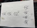
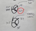
I’ve replaced all of the resistors and diodes (not just because but because they were out of spec). App the transistors currently test good and are closely matched. Output is barely anything unless you turn it up all the way you can hear very scratchy sounds only in the loud notes. Almost sounds like random farting. 2 transistors are getting hot and will most likely burn up if ran longer than 20 seconds. Here are my voltages they are a little off especially the driver collector that I have circled is 3 volts off.

I’m also curious about the bias circuit and how it works.
IMG_1345.jpegIMG_1344.jpeg
 
Register to hide this ad
What did you replace the output section diodes with?
Ma20 transistors. Here’s the link that was copied from the internet.
 
The bias to X11R/X12R looks a bit high. Double check that you have D3R installed correctly. Measure the voltage *across* D2R and D3R.
 
The bias to X11R/X12R looks a bit high. Double check that you have D3R installed correctly. Measure the voltage *across* D2R and D3R.
What voltages do you think I should see? I’m going to put a 500ohm potentiometer in place of the 100 ohm resistors as per the advice of buck to try to adjust the bias
 
What I really don’t understand is why the diagram isn’t a mirror image of itself on the positive and negative sides. The positive seems straight forward but the negative side seems to be directly connected to the output from the base of x10r. Its confusing for sure.
 
Should see between 0.2 and 0.3 volts across those 'diodes'.

X10R and X12R are the actual output transistors. X9R and X11R are bootstrapped to the output to control the collector voltage on the output transistors. Effectively this causes about half the buss voltage to be dropped across each transistor so they share the load. Changing that 100 ohm resistor will unbalance that,but it is worth a try.
 
Should see between 0.2 and 0.3 volts across those 'diodes'.

X10R and X12R are the actual output transistors. X9R and X11R are bootstrapped to the output to control the collector voltage on the output transistors. Effectively this causes about half the buss voltage to be dropped across each transistor so they share the load. Changing that 100 ohm resistor will unbalance that,but it is worth a try.
So with the 100ohm resistors in I’ve got .33 volts across each diode. I’ve been measuring the voltage across the emitter resistors and I’m getting about 70mv. I put a potentiometer where the 100ohm was and found that when I get my base voltages to 17 and -17 as per the diagram I’m getting 70mv across the emitter resistors which seems high.
 
Screenshot 2024-02-20 120713.jpg
Is that 18.4 or 18.7?

Germaniums are so variable as to the B-E voltage that it is sometimes hard to tell if the device is good or not from the Vbe. How did you test them?
 
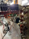
That’s 18.4. I’m testing them with a handheld tester. I’ve tried different combos of transistors and the lower one still gets hot. I’m drawing .09v through the emitter resistor. I’ve put some adjustable pots where the 100ohm resistors are to experiment and I can get the voltage at the base of x11r to go from 10-20v but still no change in current through the emitter resistor and the transistor still gets hot. image.jpgimage.jpg
 
If that one transistor is not on the heat sink, I'm not surprised if it gets hot. The voltage from the base to emitter of X12R should be the same as the B-E voltage of X10R. The voltage across X12R emitter resistor should be the same as the voltage across X10R's emitter resistor. The voltage at X11R collector should be very near 0. I'm still suspicious of a bad X12R. When you say you've tried different combos of transistors, what exactly do you mean?
 
Yes it’s off the heat sink until I can get the voltages right. I have a bunch of to-3 germanium pnp transistors that I’ve been matching and trying. I was thinking a bad x12 too. At this point it’s the only thing that makes sense. The voltage at 11x is about 1.5 to 2v which was putting dc onto the speaker outputs but I tested a junk speaker and the voltage goes away and the speaker doesn’t react so I think it low current. The voltage across both emitter resistors is the same but they’re both high at 90mv.

Do you think the transistor will get too hot to touch at idle off the heat sink?
 
90 mV across 0.5 ohm resistor is 180 mA. The drop across either transistor is about 17 volts, so each transistor will be dissipating 17 x 0.18 = 3.1 watts. Yes they will get hot. Put them back on the heat sink and see if X11R and X12R still get hotter than X10R & X11R. 180 mA idle current seems a bit high, but this may be designed to operate closer to class A than Class AB and it could be normal. If when all the transistors are on the heat sink and if you have the same voltage drop across both emitter resistors, the output section is probably running OK.

The actual problem could be in the driver section. The voltages in the driver section are not too far off. Have you replaced C30 & C31? Those would be possible suspects.
 
90 mV across 0.5 ohm resistor is 180 mA. The drop across either transistor is about 17 volts, so each transistor will be dissipating 17 x 0.18 = 3.1 watts. Yes they will get hot. Put them back on the heat sink and see if X11R and X12R still get hotter than X10R & X11R. 180 mA idle current seems a bit high, but this may be designed to operate closer to class A than Class AB and it could be normal. If when all the transistors are on the heat sink and if you have the same voltage drop across both emitter resistors, the output section is probably running OK.

The actual problem could be in the driver section. The voltages in the driver section are not too far off. Have you replaced C30 & C31? Those would be possible suspects.
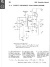
Yes those were replaced with nichicon muse 470uf. I’ll put everything back together tomorrow and see what happens. I do believe this was a class an amplifier design. This is the schematic from the 1964 rca transistor manual provided by buck.
 

Attachments

  • IMG_1427.jpeg
    IMG_1427.jpeg
    78.2 KB · Views: 4
Yes, that is the same topology. On yours, the second set of 'cascode' connected transistors is just to distribute the dissipation.
 
Power supply? If you have a scope, might want to check that all the power supply voltages are clean. Without a scope, confirm with your meter that the voltages are stable - switch the meter to an AC range and be sure there is no AC component on the power rails.
 
I did rebuild the power supply new diodes and larger capacitors. Seems to be steady but I didn’t check for ac ripple. I didn’t get a chance to work on it today but I think I’m going to put the heat sinks back in and test it again with the correct bias voltages. I didn’t measure the B to E Voltages yet that should show something
 
got it back together with the heat sinks on and the transistors barely get warm now but the sound is still awful. It will only make noise about 50% volume and then all you hear is the loud notes very distorted. It’s almost like something isn’t let the signal through.
 
Do you have an oscilloscope? Or an audio signal generator of any sort (looking for 1KHz, 0 - 1 V or so)?
 
Back
Top Bottom